GR712RC-UM, Jun 2017, Version 2.9 60 www.cobham.com/gaisler
GR712RC
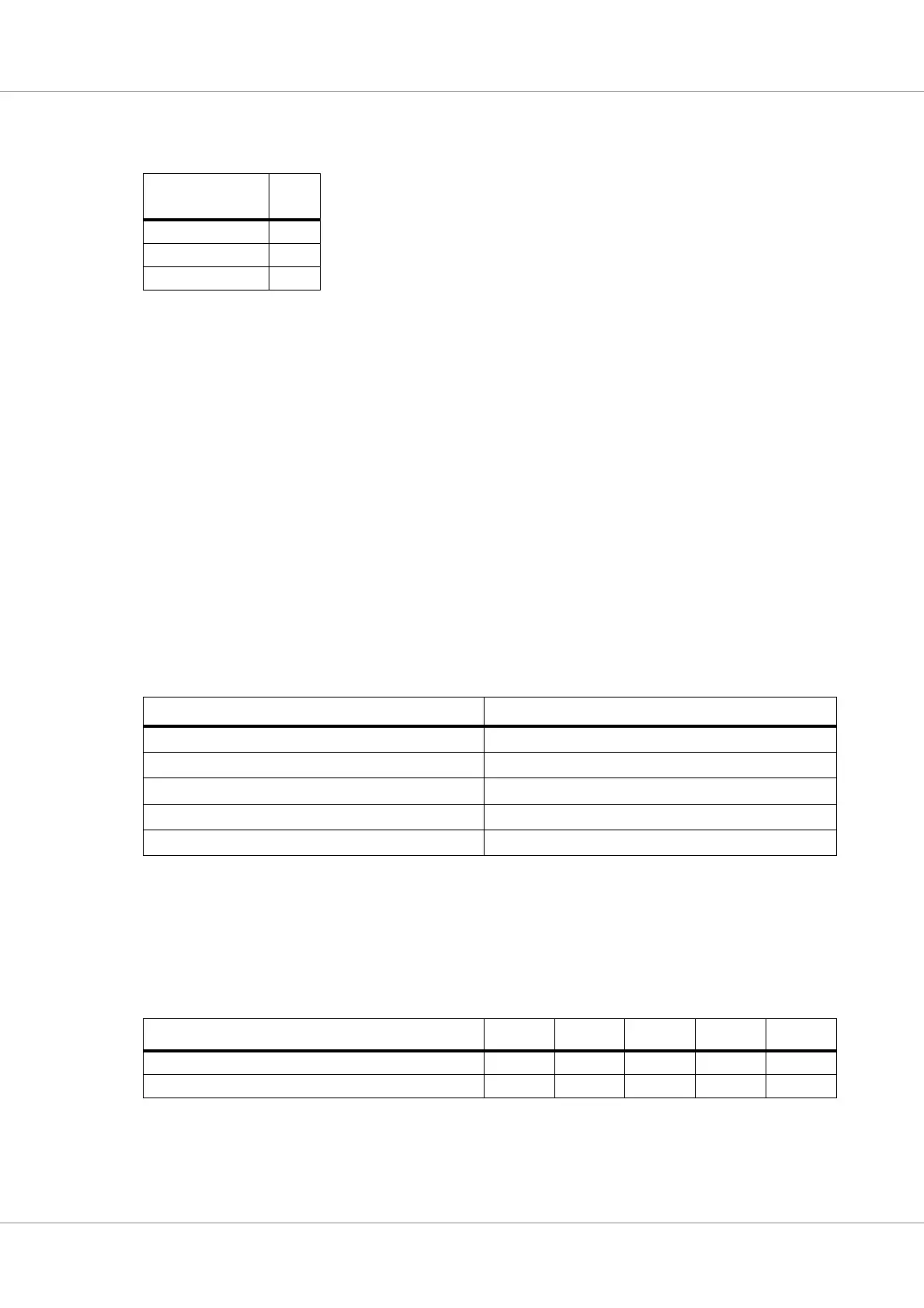
The supported combinations of width and EDAC for the SDRAM is given in table 25.
5.8.2 Address mapping
The two SDRAM chip-select signals are decoded. The SDRAM is mapped in address range
0x60000000 - 0x80000000 when the SRAM is enabled. When the SRAM disable bit is set, all access
to SRAM is disabled and the SDRAM banks are mapped in address range 0x40000000 - 0x80000000.
5.8.3 Initialisation
When the SDRAM controller is enabled, it automatically performs the SDRAM initialisation
sequence of PRECHARGE, 8x AUTO-REFRESH and LOAD-MODE-REG on both banks simultane-
ously. The controller programs the SDRAM mode register to use single location access on write and
length 8 line burst on read.
5.8.4 Configurable SDRAM timing parameters
To provide optimum access cycles for different SDRAM devices (and at different frequencies), three
SDRAM parameters can be programmed through memory configuration register 2 (MCFG2): TCAS,
TRP and TRFCD. The value of these field affects the SDRAM timing as described in table 26.
If the TCAS, TRP and TRFC are programmed such that the PC100/133 specifications are fulfilled,
the remaining SDRAM timing parameters will also be met. The table below shows typical settings for
100 and 133 MHz operation and the resulting SDRAM timing (in ns).
It should be noted that the maximum SDRAM frequency of 100 and 133 MHz is not possible with
GR712RC.
5.9 Refresh
The SDRAM controller contains a refresh function that periodically issues an AUTO-REFRESH
command to both SDRAM banks. The period between the commands (in clock periods) is pro-
Table 25. Supported SDRAM width and EDAC combinations
SDRAM bus width
EDA
C
32 None
32+7 BCH
32+16 RS
Table 26. SDRAM programmable minimum timing parameters
SDRAM timing parameter Minimum timing (clocks)
CAS latency, RAS/CAS delay (t
CAS
, t
RCD
)TCAS + 2
Precharge to activate (t
RP
) TRP + 2
Auto-refresh command period (t
RFC
) TRFC + 3
Activate to precharge (t
RAS
) TRFC + 1
Activate to Activate (t
RC
) TRP + TRFC + 4
Table 27. SDRAM example programming (clock periods)
SDRAM settings
t
CAS
t
RC
t
RP
t
RFC
t
RAS
CL=2; TRP=0, TCAS=0, TRFC=4 28275
CL=3; TRP=0, TCAS=1, TRFC=4 38275