GR712RC-UM, Jun 2017, Version 2.9 48 www.cobham.com/gaisler
GR712RC
[26:24]: Cache associativity (SETS). Number of sets in the cache: 000 - direct mapped, 001 - 2-way associative, 010 - 3-way
associative, 011 - 4-way associative
[23:20]: Set size (SSIZE). Indicates the size (KiB) of each cache set. Size = 2
SIZE
[19]: Local ram (LR). Set if local scratch pad ram is implemented.
[18:16]: Line size (LSIZE). Indicated the size (words) of each cache line. Line size = 2
LSZ
[15:12]: Local ram size (LRSZ). Indicates the size (KiB) of the implemented local scratch pad ram. Local ram size = 2
LRSZ
[11:4]: Local ram start address. Indicates the 8 most significant bits of the local ram start address.
[3]: MMU present. This bit is set to ‘1’ if an MMU is present.
The value of the instruction cache configuration register is 0x132308e8 and the value of the data
cache configuration register is 0x1b2208f8.
4.5.6 Cache registers accesses
All cache registers are accessed through load/store operations to the alternate address space (LDA/
STA), using ASI = 2. The table below shows the register addresses:
4.5.7 Software consideration
After reset, the caches are disabled and the cache control register (CCR) is 0. Before the caches may
be enabled, a flush operation must be performed to initialized (clear) the tags and valid bits. A suitable
assembly sequence could be:
flush
set 0x81000f, %g1
sta%g1, [%g0] 2
4.6 Memory management unit
A memory management unit (MMU) compatible with the SPARC V8 reference MMU is provided in
the cache control module. For details on operation, see the SPARC V8 manual.
4.6.1 ASI mappings
See table 16 for MMU ASI mappings.
4.6.2 MMU/Cache operation
When the MMU is disabled, the caches operate as normal with physical address mapping. When the
MMU is enabled, the caches tags store the virtual address and also include an 8-bit context field. On
cache miss or access to an uncacheable location, the virtual address is translated to a physical address
before the access appears on the AHB bus.
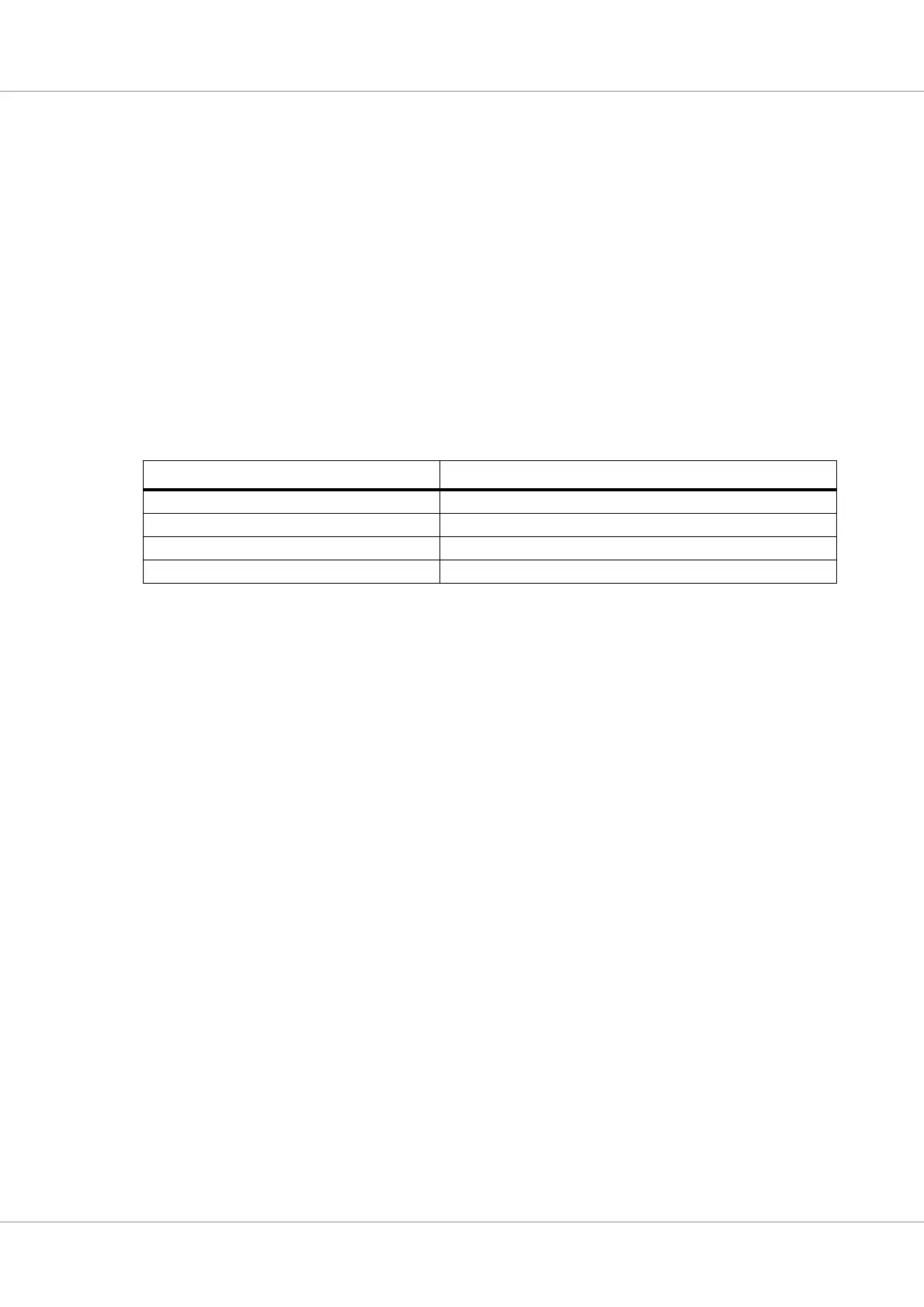
Table 19. ASI 2 (system registers) address map
Address Register
0x00 Cache control register
0x04 Reserved
0x08 Instruction cache configuration register
0x0C Data cache configuration register