GR712RC-UM, Jun 2017, Version 2.9 45 www.cobham.com/gaisler
GR712RC
4.3.2 Instruction cache tag
A instruction cache tag entry consists of several fields as shown in figure 6:
Field Definitions:
[31:12]: Address Tag (ATAG) - Contains the tag address of the cache line.
[7:0]: Valid (V) - When set, the corresponding sub-block of the cache line contains valid data. These bits are set when a
sub-block is filled due to a successful cache miss; a cache fill which results in a memory error will leave the valid
bit unset. A FLUSH instruction will clear all valid bits. V[0] corresponds to address 0 in the cache line, V[1] to
address 1, V[2] to address 2 and so on.
4.4 Data cache
4.4.1 Operation
The data cache is implemented as a 4x4 KiB multi-way cache with 16 bytes/line, using true LRU
replacement policy. Each line has a cache tag associated with it consisting of a tag field and valid field
with one valid bit for each 4-byte sub-block. On a data cache read-miss to a cachable location 4 bytes
of data are loaded into the cache from main memory. The write policy for stores is write-through with
no-allocate on write-miss. Locked AHB transfers are generated for LDD, STD, LDST and SWAP
instructions. If a memory access error occurs during a data load, the corresponding valid bit in the
cache tag will not be set. and a data access error trap (tt=0x9) will be generated.
4.4.2 Write buffer
The write buffer (WRB) consists of three 32-bit registers used to temporarily hold store data until it is
sent to the destination device. For half-word or byte stores, the stored data replicated into proper byte
alignment for writing to a word-addressed device, before being loaded into one of the WRB registers.
The WRB is emptied prior to a load-miss cache-fill sequence to avoid any stale data from being read
in to the data cache.
Since the processor executes in parallel with the write buffer, a write error will not cause an exception
to the store instruction. Depending on memory and cache activity, the write cycle may not occur until
several clock cycles after the store instructions has completed. If a write error occurs, the currently
executing instruction will take trap 0x2b.
Note: the 0x2b trap handler should flush the data cache, since a write hit would update the cache while
the memory would keep the old value due the write error.
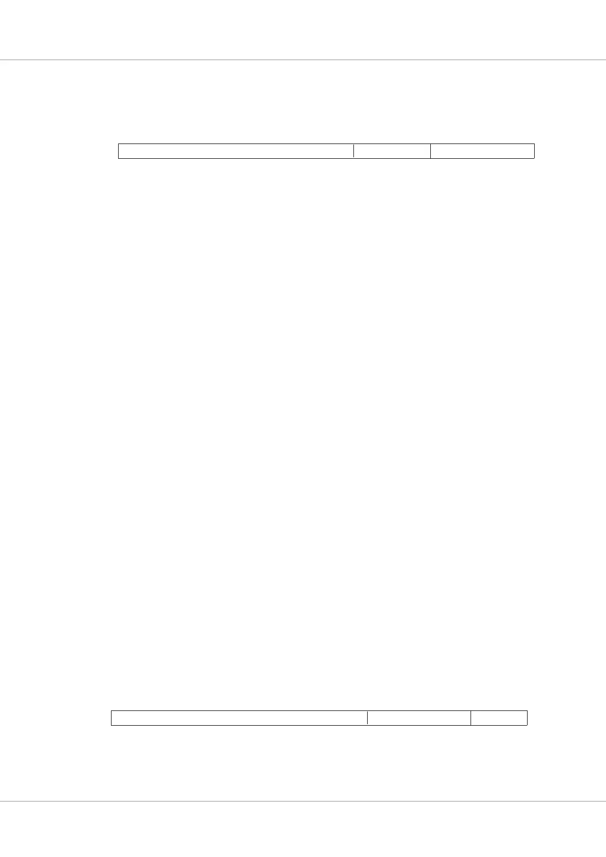
4.4.3 Data cache tag
A data cache tag entry consists of several fields as shown in figure 7:
Field Definitions:
Figure 6. Instruction cache tag layout examples
071231
VA L I DATA G
Tag for 4 KiB way, 32 bytes/line
0000
Figure 7. Data cache tag layout
031231
VA L I DATAG 000000
Tag for 4 KiB way, 16 bytes/line