GR712RC-UM, Jun 2017, Version 2.9 54 www.cobham.com/gaisler
GR712RC
5.2 PROM access
Up to two PROM chip-select signals are provided for the PROM area, ROMSN[1:0]. The size of the
banks can be set in binary steps from 16KiB to 16MiB. The total maximum supported PROM capac-
ity is 32 MiB.
A read access to PROM consists of two data cycles and between 0 and 30 waitstates. The read data
(and optional EDAC check-bits) are latched on the rising edge of the clock on the last data cycle. On
non-consecutive accesses, a lead-out cycle is added after a read cycle to prevent bus contention due to
slow turn-off time of PROM devices. Figure 16 shows the basic read cycle waveform (zero waitstate)
for non-consecutive PROM reads. Note that the address is undefined in the lead-out cycle. Figure 17
shows the timing for consecutive cycles (zero waitstate). Waitstates are added by extending the data2
phase. This is shown in figure 18 and applies to both consecutive and non-consecutive cycles. Only an
even number of waitstates can be assigned to the PROM area.
The PROM area will wrap back to the first bank after the end of the last decoded bank. As an exam-
ple, if the
ROMBANKSZ field is set to 13 the following banks will be decoded:
bank 0: 0x00000000 - 0x03FFFFFF
bank 1: 0x04000000 - 0x07FFFFFF
bank 2: 0x08000000 - 0x0BFFFFFF (no external select signal provided)
bank 3: 0x0C000000 - 0x0FFFFFFF (no external select signal provided)
...
bank 0 starting again at 0x10000000 (the same pattern applies for other values less than 13, addresses
will wrap after the last decoded bank).
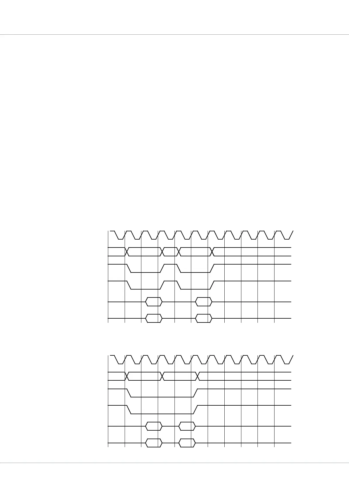
Figure 16. Prom non-consecutive read cyclecs.
data1 data2
address
romsn
data
oen
cb
data1 data2lead-out lead-out
sdclk
D1
D2
CB2CB1
A1
A2
Figure 17. Prom consecutive read cyclecs.
data1 data2
address
romsn
data
oen
cb
data2data lead-out
sdclk
A1
D2
CB2CB1
D1
A2
data1