GR712RC-UM, Jun 2017, Version 2.9 59 www.cobham.com/gaisler
GR712RC
In 8-bit mode, the PROM/SRAM devices should be connected to the most significant byte of the data
bus (DATA[31:24]). The least significant part of the address bus should be used for addressing
(ADDRESS[23:0]).
5.6 8- bit I/O access
Similar to the PROM/SRAM areas, the IO area can also be configured to 8-bits mode. However, the I/
O device will NOT be accessed by multiple 8/16 bits accesses as the memory areas, but only with one
single access just as in 32-bit mode. To access an IO device on an 8-bit bus, only byte accesses should
be used (LDUB/STB instructions for the CPU).
5.7 Burst cycles
To improve the bandwidth of the memory bus, accesses to consecutive addresses can be performed in
burst mode. Burst transfers will be generated when the memory controller is accessed using an AHB
burst request. These includes instruction cache-line fills, double loads and double stores. The timing
of a burst cycle is identical to the programmed basic cycle with the exception that during read cycles,
the lead-out cycle will only occurs after the last transfer. Burst cycles will not be generated to the IO
area.
5.8 SDRAM access
5.8.1 General
Synchronous dynamic RAM (SDRAM) access is supported to two banks of PC100 compatible
devices. The SDRAM controller supports 64Mibit, 256Mibit and 512Mibit devices with 8 - 12 col-
umn-address bits, and up to 13 row-address bits. The size of the two banks can be programmed in
binary steps between 4MiB and 512MiB. The total maximum supported SDRAM capacity is 1 GiB.
The operation of the SDRAM controller is controlled through MCFG2 and MCFG3 (see below).
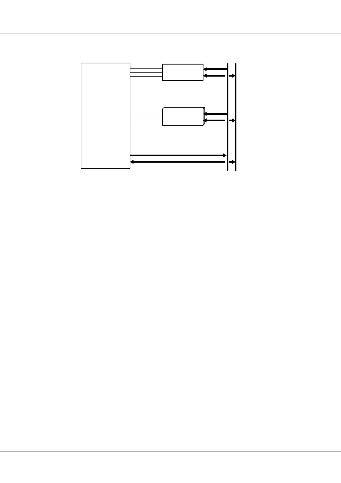
Figure 26. 8-bit memory interface example
CS
OE
WE
A
D
PROM
CS
OE
WE
A
D
SRAM
RAMSN[0]
RAMOEN
RAMWEN
ROMSN[0]
OEN
AD
MEMORY
ADDRESS[23:0]
DATA[31:24]
RWE[0]
D[31:24]
D[31:24]
A[25:0]
A[25:0]
WRITEN
8-bit PROM
8-bit RAM
CONTROLLER