GR712RC-UM, Jun 2017, Version 2.9 66 www.cobham.com/gaisler
GR712RC
5.13 Read strobe
The READ output signal indicates the direction of the current PROM,SRAM,IO or SDRAM transfer,
and it can be used to drive external bi-directional buffers on the data bus. It always is valid at least one
cycle before and after the bus is driven, at other times it is held either constant high or low.
5.14 Registers
The core is programmed through registers mapped into APB address space.
Table 28. FTMCTRL memory controller registers
APB Address offset Register
0x80000000 Memory configuration register 1 (MCFG1)
0x80000004 Memory configuration register 2 (MCFG2)
0x80000008 Memory configuration register 3 (MCFG3)
0x8000000C Memory configuration register 4 (MCFG4)
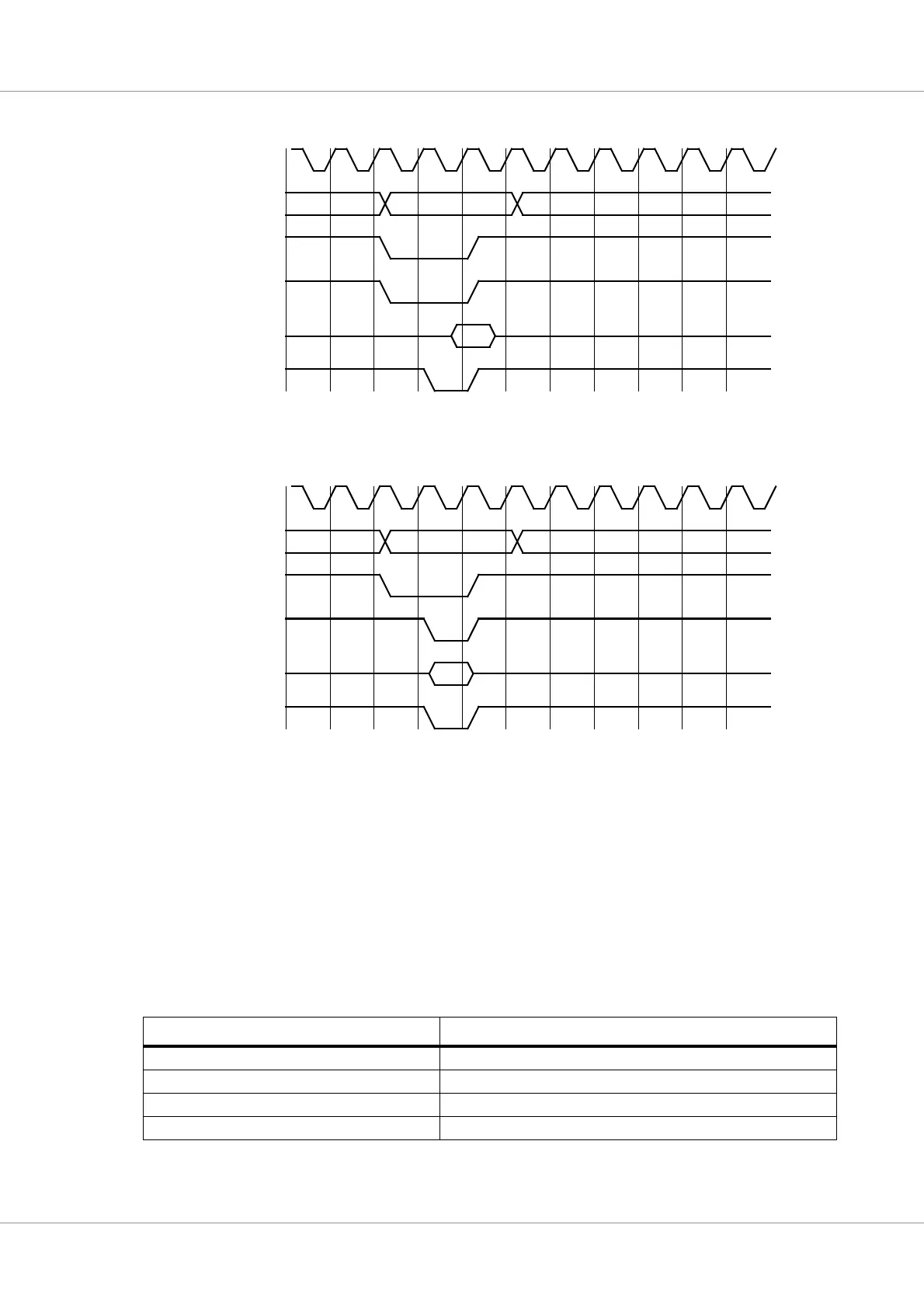
Figure 30. Read cycle with BEXCN.
data1 data2
address
romsn/iosn/ramsn
data
oen
lead-out
sdclk
D1
A1
bexcn
Figure 31. Write cycle with BEXCN. Chip-select (iosn) is not asserted in lead-in cycle for io-accesses.
lead-in data2
address
romsn/iosn/ramsn
data
rwen
lead-out
sdclk
D1
A1
bexcn