GR712RC-UM, Jun 2017, Version 2.9 57 www.cobham.com/gaisler
GR712RC
5.4 SRAM access
The SRAM area is divided on two RAM banks. The size of the banks (RAMSN[1:0]) is programmed
in the RAM bank-size field (MCFG2[12:9]) and can be set in binary steps from 8KiB to 16MiB. The
total maximum supported SRAM capacity is 32 MiB. A read access to SRAM consists of two data
cycles and between zero and three waitstates. The read data (and optional EDAC check-bits) are
latched on the rising edge of the clock on the last data cycle. On non-consecutive accesses, a lead-out
cycle is added after a read cycle to prevent bus contention due to slow turn-off time of memories. Fig-
ure 23 shows the basic read cycle waveform (zero waitstate). Waitstates are added in the same way as
for PROM in figure 18.
For read accesses to RAMSN[1:0], a shared output enable signal (RAMOEN) is provided. A write
access is similar to the read access but takes a minimum of three cycles. Waitstates are added in the
same way as for PROM.
The GR712RC uses a common SRAM write strobe (RAMWEN), and the read-modify-write bit
MCFG2 must be set to enable read-modify-write cycles for sub-word writes.
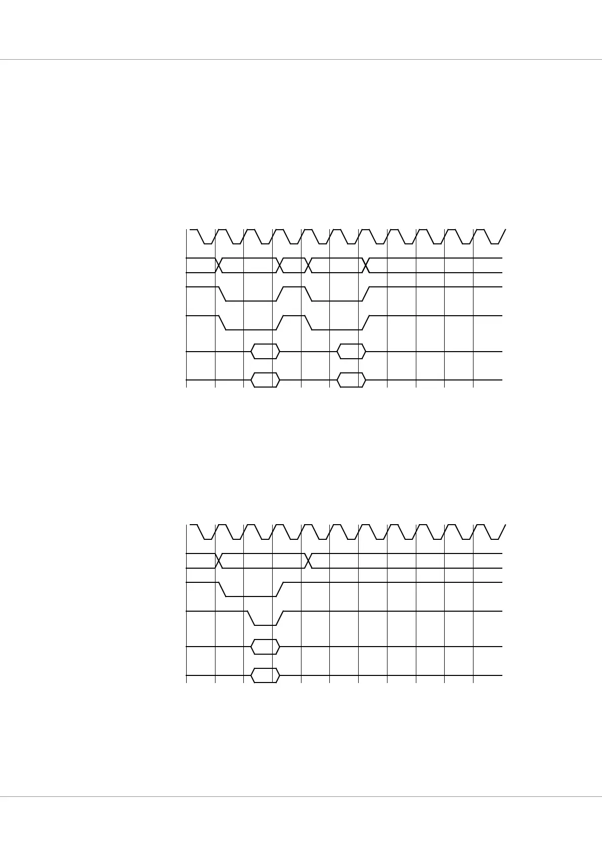
Figure 23. Sram non-consecutive read cyclecs.
data1 data2
address
ramsn
data
cb
data1 data2lead-out lead-out
sdclk
D1
D2
CB2CB1
A1
A2
ramoen
Figure 24. Sram write cycle (0-waitstates)
data
address
ramsn
data
ramwen
cb
lead-out
sdclk
A1
D1
CB1
lead-in