GR712RC-UM, Jun 2017, Version 2.9 51 www.cobham.com/gaisler
GR712RC
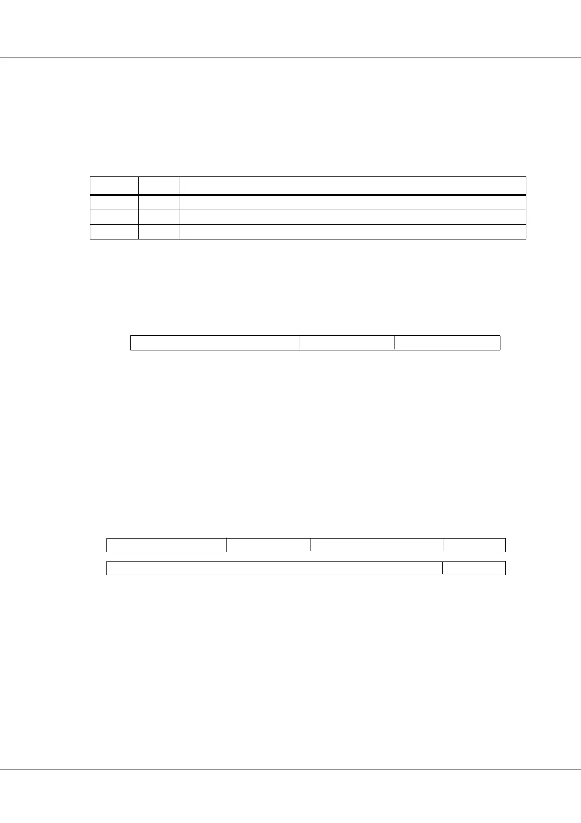
[15:14]: IU FT ID - Defines which error protection is implemented. Hardcoded to “11”.
[13:11]: IU RF error counter - Number of detected errors in the IU register file.
[10:3]: RF Test bits (FTB) - In test mode, these bits are xored with correct checkbits before written to the register file.
[2]: DP ram select (DP) - See table below for details.
[1]: IU RF Test Enable - Enables register file test mode. Checkbits are xored with TB before written to the register file.
[0]: IU RF protection disable (IDI) - Disables IU register file protection when set.
4.8.3 Register file EDAC/parity bits diagnostic read-out
The register file checkbits can be read out through the DSU address space at 0x90300800. The check-
bits are read out for both read ports simultaneously as defined in the figure below:
4.8.4 Cache error protection
Each word in the cache tag and data memories is protected by four check bits. An error during cache
access will cause a cache line flush, and a re-execution of the failing instruction. This will insure that
the complete cache line (tags and data) is refilled from external memory. For every detected error, a
counter in the cache control register is incremented. The counters saturate at their maximum value (3),
and should be reset by software after read-out.
The context and parity bits for data and instruction caches can be read out via ASI 0xC - 0xF when the
PS bit in the cache control register is set. The data will be organized as shown below:
4.8.5 Data scrubbing
There is generally no need to perform data scrubbing on either IU register file or the cache memory.
During normal operation, the active part of the IU register files will be flushed to memory on each
task switch. This will cause all registers to be checked and corrected if necessary. Since most real-time
operating systems performs several task switches per second, the active data in the register file will be
frequently refreshed.
The similar situation arises for the cache memory. In most applications, the cache memory is signifi-
cantly smaller than the full application image, and the cache contents is gradually replaced as part of
normal operation. For very small programs, the only risk of error build-up is if a part of the applica-
Table 22. DP ram select usage
ITE DP Function
1 0 Write to IU register (%i, %l, %o, %g) will only write location of %rs1
1 1 Write to IU register (%i, %l, %o, %g) will only write location of %rs2
0 X IU registers written nominally
Figure 13. Register file checkbits read-out layout
RF ECC Port 2
RESERVED
16
0
7
RF ECC port 1
8
31
Figure 14. Data cache tag diagnostic access when CCR.PS = ‘1’
04
3
31
TAG PAR[3:0]
ASI = 0xC
MMU CTX [7:0]
ASI = 0xD
16
15
23
DATA PAR[3:0]
ASI = 0xE
ASI = 0xF