RM0453 Rev 2 421/1454
RM0453 General-purpose I/Os (GPIO)
426
10.4.31 GPIOH alternate function low register (GPIOH_AFRL)
Address offset: 0x1C20
Reset value: 0x0000 0000
Bits 31:17 Reserved, must be kept at reset value.
Bit 16 LCKK: Lock key
This bit can be read any time. It can only be modified using the lock key write sequence.
0: Port PH configuration lock key not active
1: Port PH configuration lock key active. GPIOH_LCKR is locked until the next MCU reset or
peripheral reset.
LOCK key write sequence:
WR LCKR[16] = 1 + LCKR[15:0]
WR LCKR[16] = 0 + LCKR[15:0]
WR LCKR[16] = 1 + LCKR[15:0]
RD LCKR
RD LCKR[16] = 1 (This read operation is optional but it confirms that the lock is active.)
Note: During the LOCK key write sequence, the value of LCK[15:0] must not change.
Any error in the lock sequence aborts the lock.
After the first lock sequence on any bit of the port, any read access on the LCKK bit
returns 1 until the next MCU reset or peripheral reset.
Bits 15:4 Reserved, must be kept at reset value.
Bit 3 LCK3: Port PH3 lock configuration
This bit is read/write but can only be written when the LCKK bit is 0.
0: Port PH3 configuration not locked
1: Port PH3 configuration locked
Bits 2:0 Reserved, must be kept at reset value.
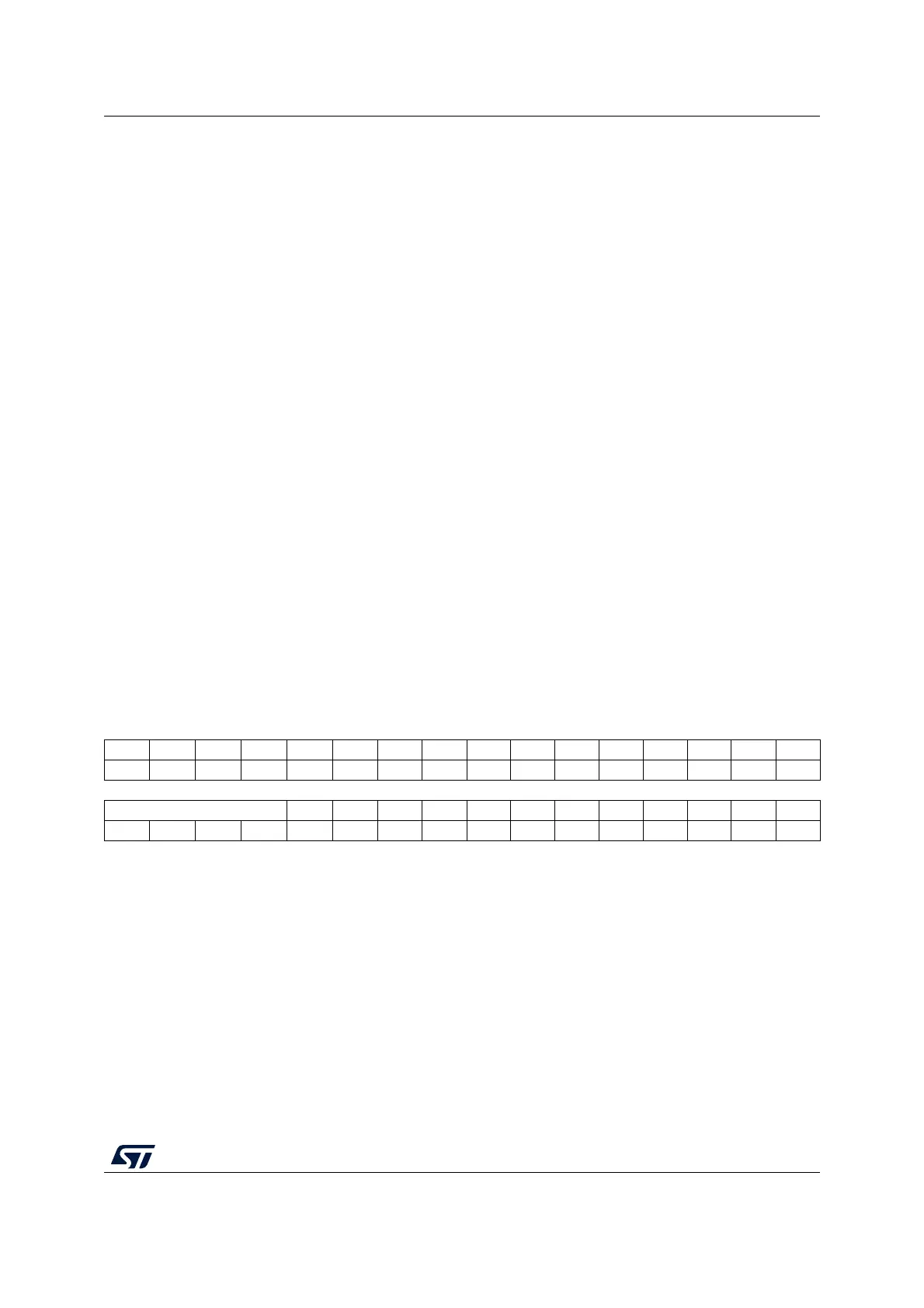
31 30 29 28 27 26 25 24 23 22 21 20 19 18 17 16
Res. Res. Res. Res. Res. Res. Res. Res. Res. Res. Res. Res. Res. Res. Res. Res.
1514131211109876543210
AFSEL3[3:0] Res. Res. Res. Res. Res. Res. Res. Res. Res. Res. Res. Res.
rw rw rw rw
Bits 31:16 Reserved, must be kept at reset value.
Bits 15:12 AFSEL3[3:0]: Port PH3 alternate function selection
These bits are written by software to configure alternate function I/Os.
0x0: AF0 selected
0x1: AF1 selected
0x2: AF2 selected
...
0xE: AF14 selected
0xF: AF15 selected
Bits 11:0 Reserved, must be kept at reset value.

 Loading...


