CA-500 Series S/M 3-20 Revised December 2001
8
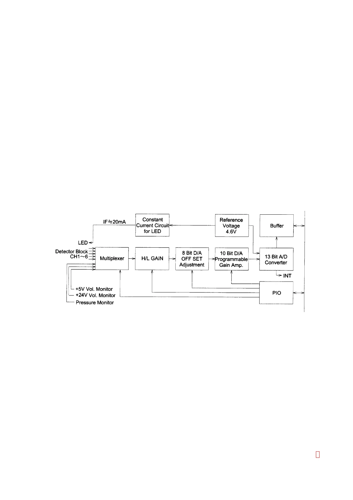
(16) Detector Block Interface (U515, 506, 514, 502, 513, 505, 501)
This circuit sends the various commands such as the switching command for the signals from
Detector Block (scattered light 1CH ~ 4CH, transmitted light 5CH, transmitted light for Immunoassy
6CH), the H/L Gain Amplifier command, Offset voltage control command, Gain voltage control
command, and the A-D converting command. Also, the interface circuit drives the LED which is the
light source of Detector Block with the constant current. Switching of each channel signal is
performed every 20 ms by the multiplexer (U515) control command and then the procedure for the
selected signal is performed.
By the H/L Gain Amplifier (U506-1, 2, 3 pin, U-514), switching between high sensitivity and low
sensitivity in the [Detector Block Adjustment] on the Service mode is performed.
The signal of the Offset voltage control circuit (U502, U505-8, 9, 10) composed by 8 Bit D/A converter
and OP Amplifier is added on the above signal.
In addition, the Gain voltage control is performed at the programmable gain amplifier (U513, U505-5,
6, 7) composed by 10 Bit D/A converter and the OP amplifier.
Both the Offset control value and the Gain control value are adjusted by the [Detector Block
Adjustment] on the Service mode and stored in the EEPROM.
LED ON/OFF is executed by controlling 20 mA constant current circuit of U506 for 1CH ~ 5CH, and
the photo-coupler (PC1) of PCB No. 2157 on Detector Block for 6CH.
These adjusted values are converted to the digital signals by the 13 Bit A/D converter (U501).
Additionally, as the signals other than the signals of Detector Block, +5 V, +24 V voltage level signals
and the pressure sensor signal are entered, which enables the voltage monitoring and the pressure
indication.
Figure 3-12:
Detector Block Interface