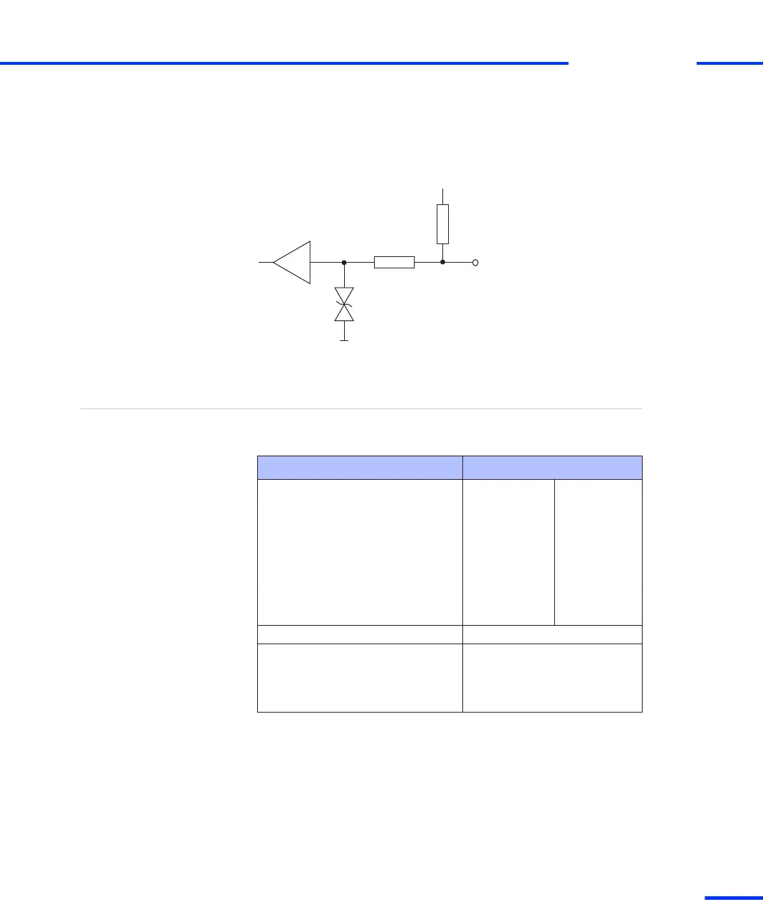
Up to board revision DS1103‑07 the I/O circuit shown above is valid
for all signals of the slave DSP I/O unit. As of board revision
DS1103‑09 the I/O circuit of some signals has changed (see below).
1 kΩ
10 kΩ
VCC
SADCH3 ... SADCH8
SADCH11 ... SADCH16
SPDPINT, STINT1
As of board revision
DS1103-09
→
I
All pins provide overvoltage protection circuits by using suppressor
diodes. They short‑circuit external voltage spikes above 6 V to
ground.
The slave DSP I/O have output/input levels with the following
characteristics.
Electrical characteristics
Parameter Value
Min. Max.
ADC input voltage 0 V +5.0 V
Input voltage High
Low
2.0 V
0 V
5.0 V
0.8 V
Output voltage High
Low
2.4 V
0 V
5.0 V
0.4 V
Output current ±13 mA
Input current
1)
500 μA
Input resistance 10 kΩ pull‑up to 5 V)
Power-up default All I/O channels are set to
input mode and to a defined
logical high level by the built-in
10 kΩ pull-up resistors.
1)
The current direction is shown in the circuit diagram above.
s
Slave DSP Bit I/O
t
DS1103 Hardware Installation and Configuration November 2014
173
t