Memory Interface Routing
R
100 Intel
®
Pentium
®
4 Processor / Intel
®
850 Chipset Family Platform Design Guide
The following is an example calculation for a board where ε
r
is 4.2 and thickness of prepreg is 4.5.
Note these numbers will vary with differences in prepreg thickness.
Table 24. Copper Tab Area Calculation
Layer Dielectric
Thickness
Separation
Between Signal
Traces & Copper
Tab
Minimum
Ground
Flood
Air Gap
Between
Signal &
GND Flood
Compensating
Capacitance in
Cplate (pF)
1
CTAB
Area in
sq mils
Top 4.5 6 10 6 0.8 ~3460
Inner 1 4.5 6 10 6 0.9 ~3900
Inner 2 4.5 6 10 6 1.23 ~5300
Bottom 4.5 6 10 6 1.35 ~5800
NOTE:
1
These numbers are based on a six layer stack-up.
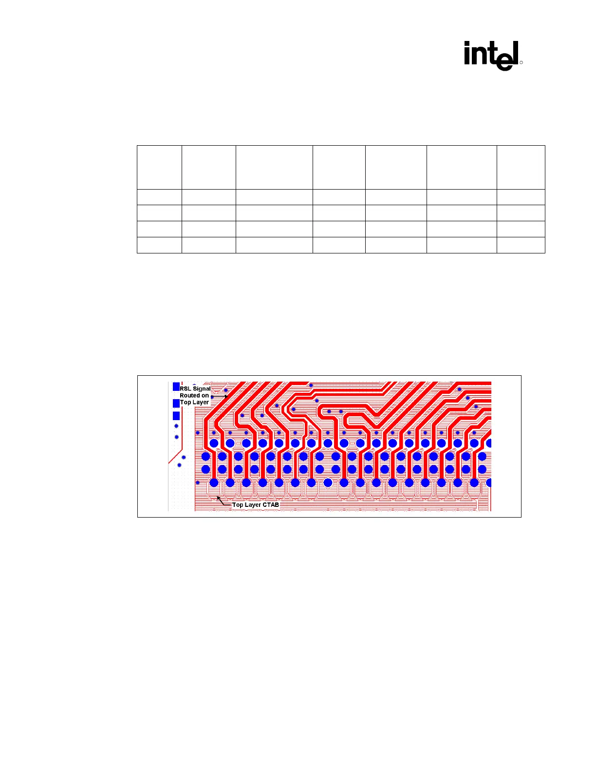
Note that more than one copper tab shape may be used as shown in the following figures. The
dimensions are based on copper area over the ground plane. The actual length and width of the
tabs may be different due to routing constraints (e.g., if tab must extend to center of hole or anti-
pad). The following figures show a routing example of tab compensation capacitors. Note, the
capacitor tabs must not interrupt ground floods around the RIMM connector pins, and they must
be connected to avoid discontinuity in the ground plane as shown.
Figure 62. Top Layer CTAB with RSL Signal Routed on the Same Layer (Ceff = 0.8 pF)