AGP Interface Routing
R
Intel
®
Pentium
®
4 Processor / Intel
®
850 Chipset Family Platform Design Guide 117
7.1.4 I/O Decoupling Guidelines
A minimum of six 0.01 µF capacitors are required for I/O decoupling. The designer should evenly
distribute placement of decoupling capacitors among the AGP interface signal field and placed as
close to the MCH as possible (no further than 0.15 inches from the edge of the MCH package). It
is recommended that the designer use a low ESL ceramic capacitor, such as a 0603 body type,
X7R dielectric.
To help lower the inductive path from the decoupling capacitor, pour a solid VSS plane under the
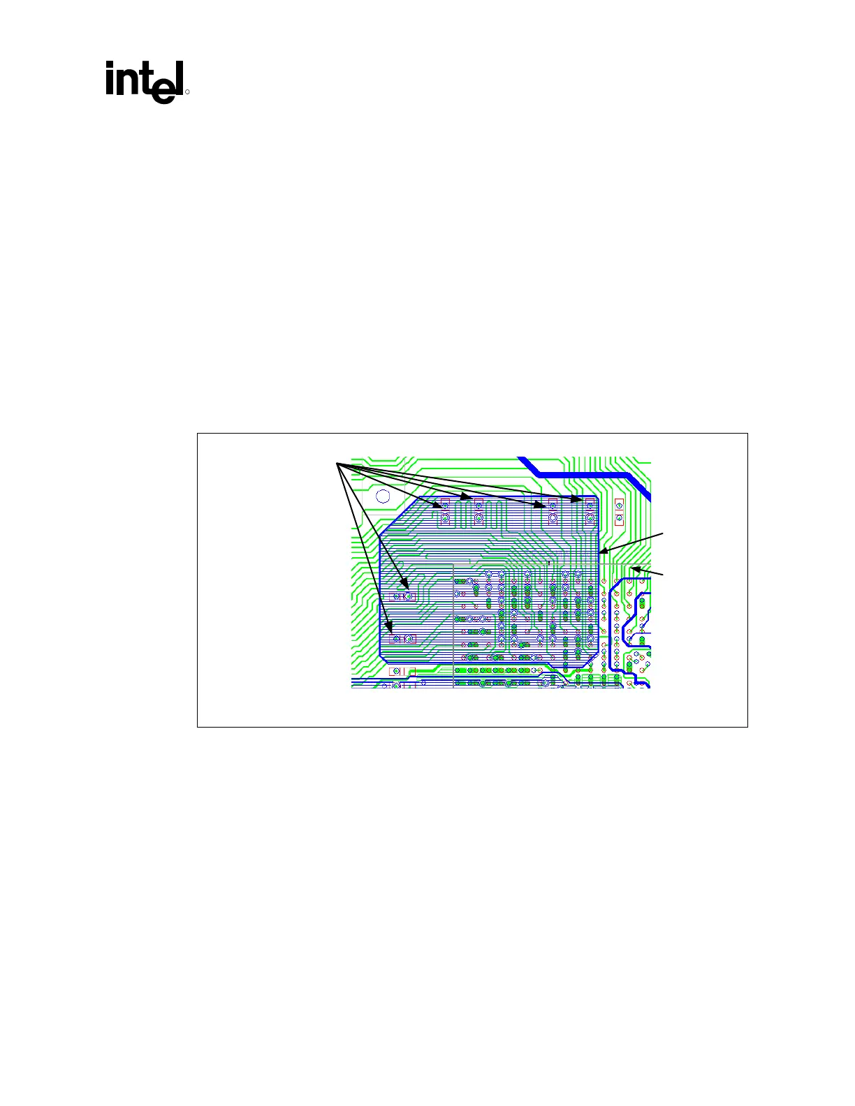
VDDQ plane on layer 3 from the decoupling capacitors to the MCH. Figure 76 illustrates an
example AGP decoupling layout with a VSS flood. This VSS flood that is referenced to VDDQ
optimizes the mutual inductance between the two planes. The mutual inductance helps cancel out
the self inductance from the power balls on the package to the decoupling caps.
Figure 76. AGP I/O Decoupling Example with a VSS Flood to Improve Power Delivery to the
Intel
®
MCH
Vss fload
on layer 3
MCH
I/O decoupling
capacitors placed within
0.150" of the MCH
In addition to the minimum decoupling capacitors, the designer should place bypass capacitors at
vias that transition AGP signal from one reference signal plane to another. One extra 0.01 µF
capacitor is required per 10 vias. The capacitor should be placed as close to the center of the via
field as possible.
The designer should ensure that the AGP connector is well decoupled as described in the revision
1.0 of the AGP Design Guide, Section 1.5.3.3.