Platform Clock Routing Guidelines
R
52 Intel
®
Pentium
®
4 Processor / Intel
®
850 Chipset Family Platform Design Guide
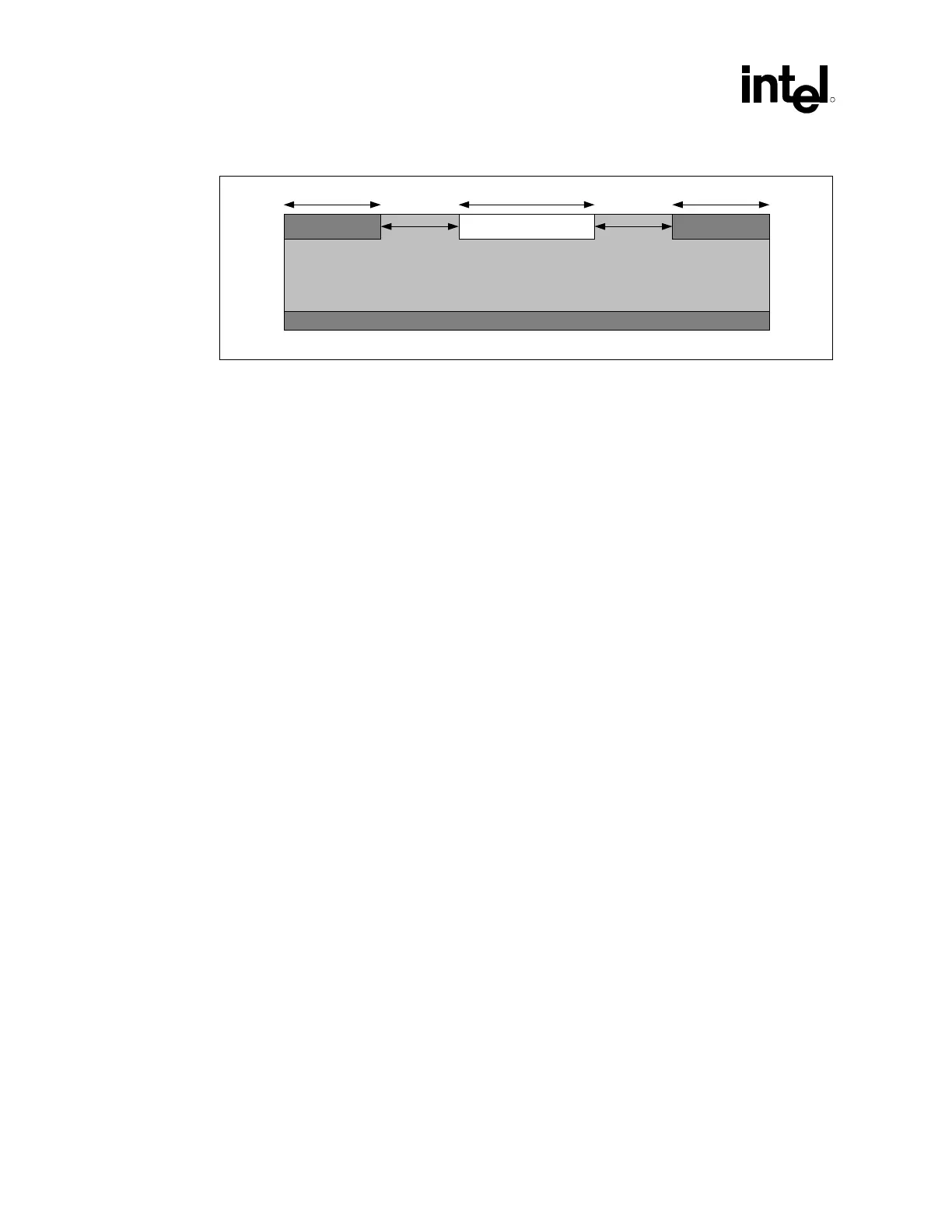
Figure 22. Non-Differential Clock Routing
GROUND CLOCK GROUND
GROUND/POWER PLANE
10 mils 10 mils18 mils
6 mils 6 mils
NonDiff-clk_route
NOTE: “CLOCK” stands for the signals CTM, CTM#, CFM and CFM#.
Note: The CTM/CTM# and CFM/CFM# clock signals must be ground referenced (with continuous
ground island/plane) at all times.
4.3.3.2 Topology Considerations
Package trace compensation, via compensation and RSL signal layer alteration must also be
considered when routing the RDRAM device clocks. Additionally, 0.021 inches of CLK per 1 inch
of RSL trace length must be added to compensate for the clock’s faster trace velocity when routing
on microstrip layers.
• For clock routing section ‘A’, the CTM/CTM# and CFM/CFM# clocks must be length
matched within ±2 mils to the RSL channel trace length. Exact matching is preferred.
• For clock routing section ‘B’, the CTM/CTM# and CFM/CFM# clocks must be length
matched within ±2 mils to the RSL channel trace length. Exact matching is preferred.
• For trace section ‘C’, the CFM/CFM# clocks must be length matched within ±2 mils to the
RSL channel trace length. Exact matching is preferred.
• For trace section ‘D’, the CTM/CTM# clocks must be length matched within ±2 mils to the
RSL channel trace length. Exact matching is preferred.
4.3.3.3 Rambus RDRAM* Device ClockTermination
300/400 MHz RDRAM technology:
The CFM/CFM# differential pair signals require termination using either 27 Ω 1% or 28 Ω 2%
resistors and a 0.1 µF capacitor as shown in Figure 23.
533 MHz RDRAM technology:
The CFM/CFM# differential pair signals require termination using 27 Ω 1% resistors and a 0.1 µF
capacitor as shown in Figure 24.