AGP Interface Routing
R
Intel
®
Pentium
®
4 Processor / Intel
®
850 Chipset Family Platform Design Guide 113
7 AGP Interface Routing
For detailed AGP Interface functionality (protocols, rules and signaling mechanisms, etc.) refer to
the AGP Interface Specification, Revision 2.0, which can be obtained from
http://www.agpforum.org
. This design guide focuses only on specific Intel 850 chipset-based
platform recommendations.
The latest AGP Interface Specification enhances the functionality of the original AGP Interface
Specification, Revision 1.0 by allowing 4x data transfers and 1.5 V operation. In addition to these
enhancements, additional performance enhancement and clarifications, such as fast write
capability, are included in the AGP Interface Specification, Revision 2.0. The Intel 850 chipset
supports these enhanced features and 1.5 V signaling only.
The 4x mode of operation on the AGP interface provides for “quad-sampling” of the AGP AD
(Address/Data) and SBA (Side-band Addressing) buses. This means data is sampled four times
during each 66 MHz AGP clock cycle or each data cycle is ¼ of 15 ns or 3.75 ns. It is important to
realize that 3.75 ns is the data cycle time not the clock cycle time. During 2x mode, data is
sampled twice during a 66 MHz clock cycle; therefore, the data cycle time is 7.5ns. These high-
speed data transfers are accomplished using source synchronous data strobing for 2x mode and
differential source synchronous data strobing for 4x mode.
With data cycle times as small as 3.75 ns and setup/hold times of 1ns, it is important to minimize
noise and propagation delay mismatch. Noise on the data lines will cause the settling time to be
large. If the mismatch between a data line and the associated strobe is too great or there is noise on
the interface, incorrect data will be sampled. The AGP signals are broken into three groups: 1x
timing domain and 2x/4x timing domain signals. In addition, the 2x/4x timing domain signals are
divided into three sets of signals (#1–#3). All signals must meet the minimum and maximum trace
length, width and spacing requirements. The trace length matching requirements are only
applicable between the 2x/4x timing domain signal sets.
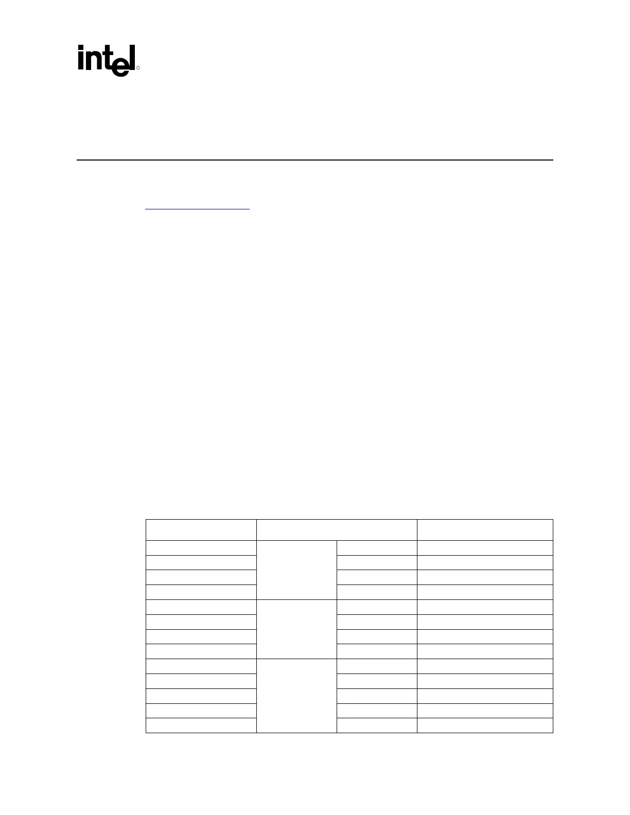
Table 25. AGP 2.0 Signal Groups
1x Timing Domain 2x/4x Timing Domain Miscellaneous Signals
CLK AD[15:0] USB+
RBF# C/BE[1:0]# USB-
WBF# AD_STB0 OVRCNT#
ST[2:0]
SET #1
AD_STB0# PME#
PIPE# AD[31:16] TYPDET#
REQ# C/BE[3:2]# PERR#
GNT# AD_STB1 SERR#
PAR
SET #2
AD_STB1# INTA#
FRAME# SBA[7:0] INTB#
IRDY# SB_STB
TRDY# SB_STB#
STOP#
DEVSEL#
SET #3