System Bus Routing
R
76 Intel
®
Pentium
®
4 Processor / Intel
®
850 Chipset Family Platform Design Guide
5.4.1.6 Topology 4: BR0# and RESET#
Since the processor does not have on-die termination on the BR0# and RESET# signals, it is
necessary to terminate using discrete components on the system board. Connect the signals
between the components as shown in Figure 41. The Intel 850 chipset has on-die termination and
thus it is necessary to terminate only at the processor end. The value of Rt should be 51 Ω ±5% for
RESET#. The value of Rt should be 150–220 Ω ±5% for BR0#.
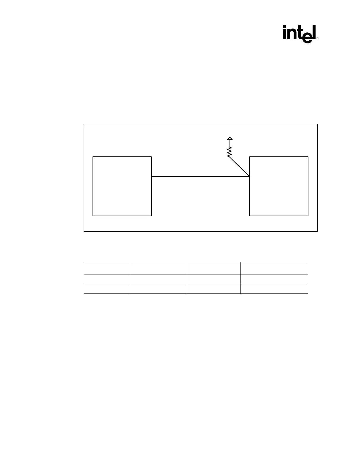
Figure 41. Routing Illustration for BR0# and RESET#
MCH Processor
L2
R
t
VCC_CPU
L1
BR0-RESET_Routing
Table 19: BR0# and RESET# Lengths
Signal Rt L1 L2
RESET# 51 Ω ≤ 1–2” 6–10”
BR0# 150–220 Ω ≤ 1–2” 6–10”
5.4.1.7 Topology 5: COMP[1:0] Signals
Terminate the COMP[1:0] pins to ground through a 51 Ω ±1% resistor as close as possible to the
pin. Do not wire COMP pins together, connect each pin to its own termination resistor.
5.4.1.8 Topology 6a: BSEL[1:0] Termination – 400 MHz System Bus Only
The BSEL[1:0] signals on the processor should be left as no-connect. The CK00 part should be
configured for 100 MHz BCLK[1:0]operation.
5.4.1.9 Topology 6b: BSEL[1:0] Termination – 533/400 MHz System Bus
The BSEL0 signal on the processor should be routed to the CK00 Sel100/133 pin. BSEL1 can be
left as a no-connect. See Figure 17.