System Bus Routing
R
Intel
®
Pentium
®
4 Processor / Intel
®
850 Chipset Family Platform Design Guide 61
5 System Bus Routing
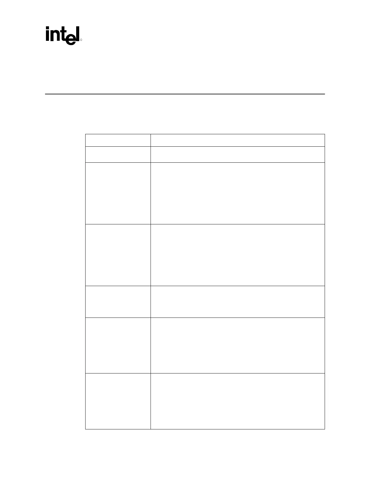
Table 10 summarizes the layout recommendations the processor configurations and expands on
specific design issues and their recommendations.
Table 10. System Bus Routing Summary for the Processor
Parameter Processor Routing Guidelines
Line to line spacing Data groups, address groups and control signals should be routed with 7 mil
traces and 13 mil spacing between traces.
Data Line lengths (a)
(agent to agent spacing)
for 82850 chipset
platforms
2 – 10 inches from pin to pin
Data signals of the same source synchronous group should be routed to the
same pad-to-pad length within ±100 mils of the median of the associated
strobes. Tighter tolerances for length matching will result in greater timing
margin for the system bus. The pad is defined as the attach point of the
silicon die to the package substrate. Signals in each source synchronous
group should be referenced to VSS. Signals within the same group may be
routed on different layers provided they are referenced to VSS and the layers
are of the same configuration (all stripline or all microstrip).
Data Line lengths (b)
(agent to agent spacing)
for 82850E chipset
platforms
2 – 8 inches from pin to pin
Data signals of the same source synchronous group should be routed to the
same pad-to-pad length within ±100 mils of the median of the associated
strobes. Tighter tolerances for length matching will result in greater timing
margin for the system bus. The pad is defined as the attach point of the
silicon die to the package substrate. Signals in each source synchronous
group should be referenced to VSS. Signals within the same group may be
routed on different layers provided they are referenced to VSS and the layers
are of the same configuration (all stripline or all microstrip).
DSTBn/p[3:0]# A data strobe and its complement should be routed within ±25 mils of the
same pad-to-pad length. The pad is defined as the attach point of the silicon
die to the package substrate.
DSTBn/p# should be referenced to VSS.
Address line lengths
(agent to agent spacing)
2 – 10 inches from pin to pin
Address signals of the same source synchronous group should be routed to
the same pad-to-pad length within ±200 mils of the associated strobe. Tighter
tolerances for length matching will result in greater timing margin for the
system bus. The pad is defined as the attach point of the silicon die to the
package substrate. A layer transition may occur if the reference plane
remains the same (VSS) and the layers are all of the same configuration (all
stripline or all microstrip).
ADSTBn/p[1:0]# 2 – 10 inches from pin to pin
Address signals of the same source synchronous group should be routed to
the same pad-to-pad length within ±200 mils of the associated strobe. Tighter
tolerances for length matching will result in greater timing margin for the
system bus. The pad is defined as the attach point of the silicon die to the
package substrate. A layer transition may occur if the reference plane
remains the same (VSS) and the layers are all of the same configuration (all
stripline or all microstrip).