AGP Interface Routing
R
Intel
®
Pentium
®
4 Processor / Intel
®
850 Chipset Family Platform Design Guide 119
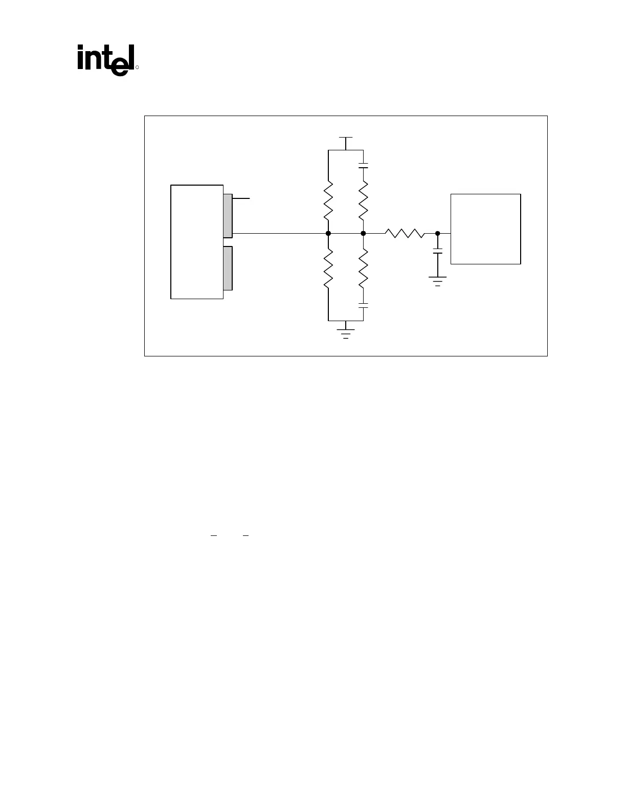
Figure 77. AGP 2.0 V
REF
Generation and Distribution for 1.5 V Cards
82 Ω 1%
GREF[1:0]
VDDQ
AGP
Add-in
Card
MCH
1 kΩ 1%
1 kΩ 1%
500 pF
500 pF
82 Ω 1%
AGP_2V_VREF_Gen
Vrefgc
Pin A66
Vrefcg
Pin B66
220–330 Ω
0.1 uF
7.1.8 Intel
®
MCH AGP Interface Buffer Compensation
The MCH AGP interface supports resistive buffer compensation (GRCOMP[1:0]). The
GRCOMP[1:0] signals must be tied to a 40 Ω ± 2% or 39 Ω ± 1% pull-down resistor to ground.
This trace should be kept to 10 mils wide and less than 0.5 inches long.
7.1.9 AGP Pull-ups/Pull-down on AGP Signals
Some of the AGP signals may require either a pull-up resistor to VDDQ (not VCC3.3) or pull-
down resistor to GND. This is to ensure stable values are maintained when agents are not actively
driving the bus. The recommended AGP pull-up/pull-down resistor value is 8.2 Ω at 10%
tolerance (4 kΩ <
R
value
< 16 kΩ). The AGP interface does not require external termination.
The trace stub length to the pull-up/pull-down resistor should be kept to a minimum to avoid
signal reflection. This trace length is different for 1x and 2x/4x modes. Below are the
recommended stub lengths for 1x and 2x/4x modes.
• 1x mode, trace stub to pull-up resistor should be kept to less than 0.5 inches
• 2x/4x mode, trace stub to pull-up resistor should be kept to less than 0.1 inches
Short stub lengths help minimize signal reflections from the stub. The strobe signals require pull-
up/pull-down on the motherboard to ensure stable values when there are no agents driving the bus.
Note: The G_GNT# and G_PAR signals require pull-ups to VDDQ.
The MCH G_GNT# output signal will be tri-stated during RSTIN# assertion. This signal must
have an external pull-up resistor to keep it from floating during the RSTIN# assertion. The
recommended value is the same as the other AGP common clock signals.