Platform Clock Routing Guidelines
R
Intel
®
Pentium
®
4 Processor / Intel
®
850 Chipset Family Platform Design Guide 55
The circuit shown is required to match the impedance of the DRCG to the 28 Ω channel
impedance. More detailed information can be found in the Direct Rambus Clock Generator
Specification.
The previously recommended 15 pF capacitors on CTM/CTM# should be removed. The 4 pF
capacitor shown in the figure should not be assembled (“no-stuff”).
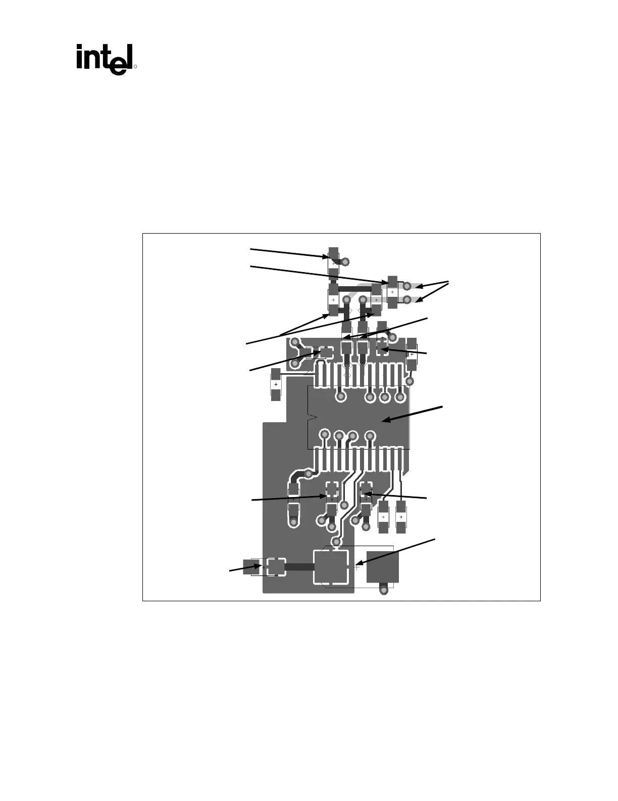
4.3.5 Rambus DRCG* Layout Example
Figure 26. Rambus DRCG* Layout Example
Rs - 39
Ω
(Keep trace from DRCG to
Rs VERY short)
Rp - 51 Ω
(Keep trace from Rs
to Rp short)
CTM/CTM# route on
bottom layer
Cmid - 100pF
EMI Cap - 4pF
Do Not Stuf
Decouplin
Cap - 0.1uF
(Place VERY Near DRCG 3.3V Pin!)
Decouplin
Cap - 0.1uF
(Place VERY Near DRCG 3.3V Pin!)
Decoupling Cap - 0.1uF
(Place VERY Near DRCG 3.3V Pin!)
Decouplin
Cap - 0.1uF
(Place VERY Near DRCG 3.3V Pin!)
Bulk Decou
lin
Ca
- 10uF
(Place Near DRCG)
Ferrite Bead
(L22 in Reference Schematics)
3.3V-DRCG Flood
Flood 3.3V-DRCG on the top layer
around DRCG. Flood MUST include:
4 DRCG Power Pins
4 0.1uF Capacitors
1 10uF Bulk Capacitor
1 Isolation Ferrite Bead