Intel® Pentium® 4 Processor in the 478-Pin Package Processor Power Distribution Guidelines
R
Intel
®
Pentium
®
4 Processor / Intel
®
850 Chipset Family Platform Design Guide 217
11.1.8 FMB1 – Common Layout Issues
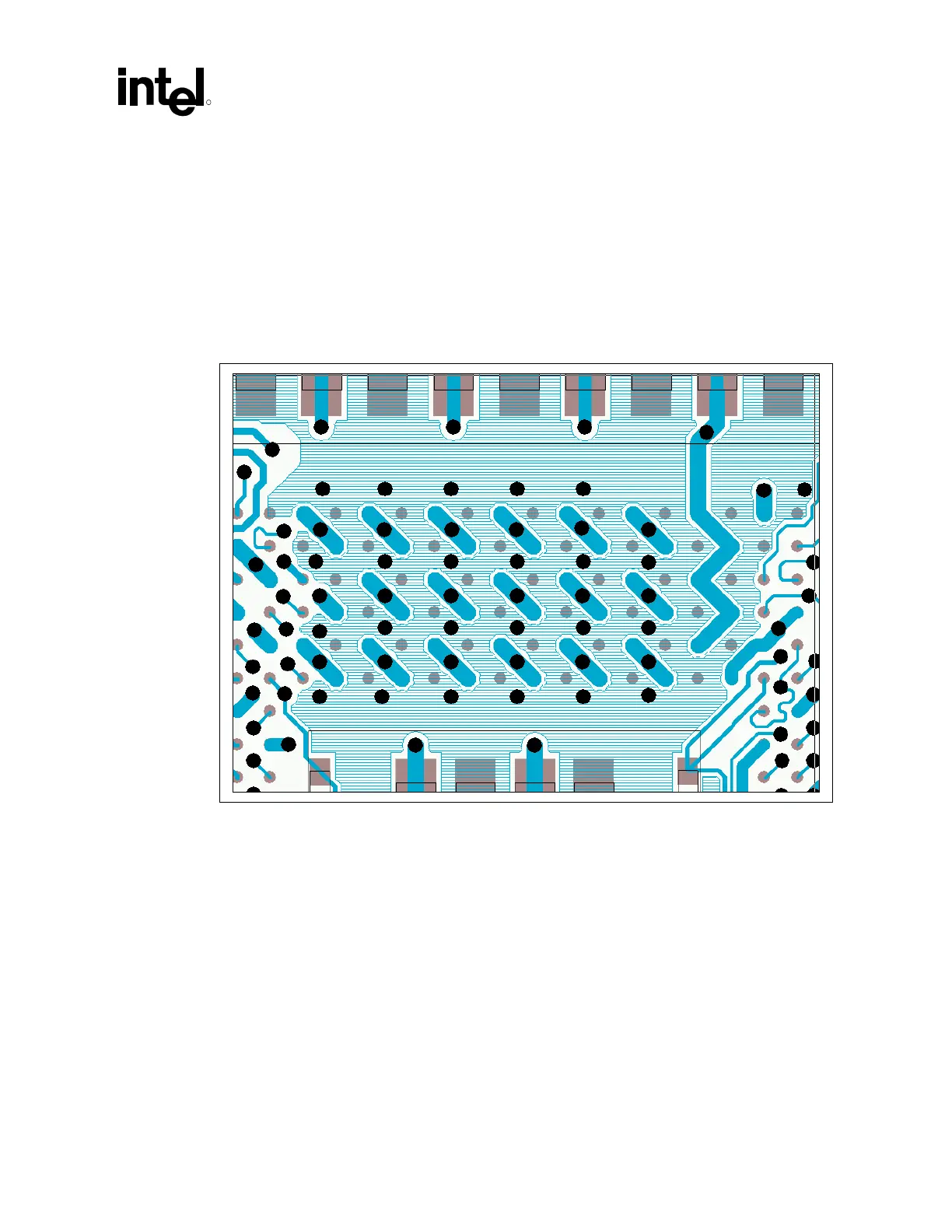
The processor socket has 478 pins with 50-mil pitch. The routing of the signals, power and ground
pins will require creation of many vias. These vias cut up the power and ground planes beneath the
processor resulting in increased inductance of these planes. In order to provide the best path
through the via field, it is recommended that vias are shared for every two processor ground pins
and for every two processor power pins. Figure 161 illustrates this via sharing.
Figure 161. Shared Power and Ground Vias
The switching voltage regulators typically used for processor power delivery require the use of a
feedback signal for output error correction. The VCC_SENSE and VSS_SENSE pins on the
processor should not be used for generating this feedback. These pins should be used as
measurement points for lab measurements only. They can be routed to a test point or via on the
back of the motherboard with a trace that is a maximum length of 100 mils for this purpose. The
socket loadline defined in the Intel
®
Pentium
®
4 Processor in the 478-pin Package VR Down
Design Guidelines is defined from pins AC14 (VCC_CPU) and AC15 (VSS) and should be
validated from these pins as well. This pins are located approximately in the center of the pin field
on the North side of the processor. Feedback for the voltage regulator controller should therefore
be taken close to this area of the power delivery shape.
Figure 162 shows an example routing of the feedback signal. It is routed as a trace from the 1206
capacitor in the Northwest corner of the processor back to the voltage regulator controller.
Because the feedback in this case is not taken from the exact point that defines the socket loadline
(pins AC14/AC15), it is important to consider any voltage drop from the feedback point to these
pins in the design.