I/O Controller Hub 2
R
160 Intel
®
Pentium
®
4 Processor / Intel
®
850 Chipset Family Platform Design Guide
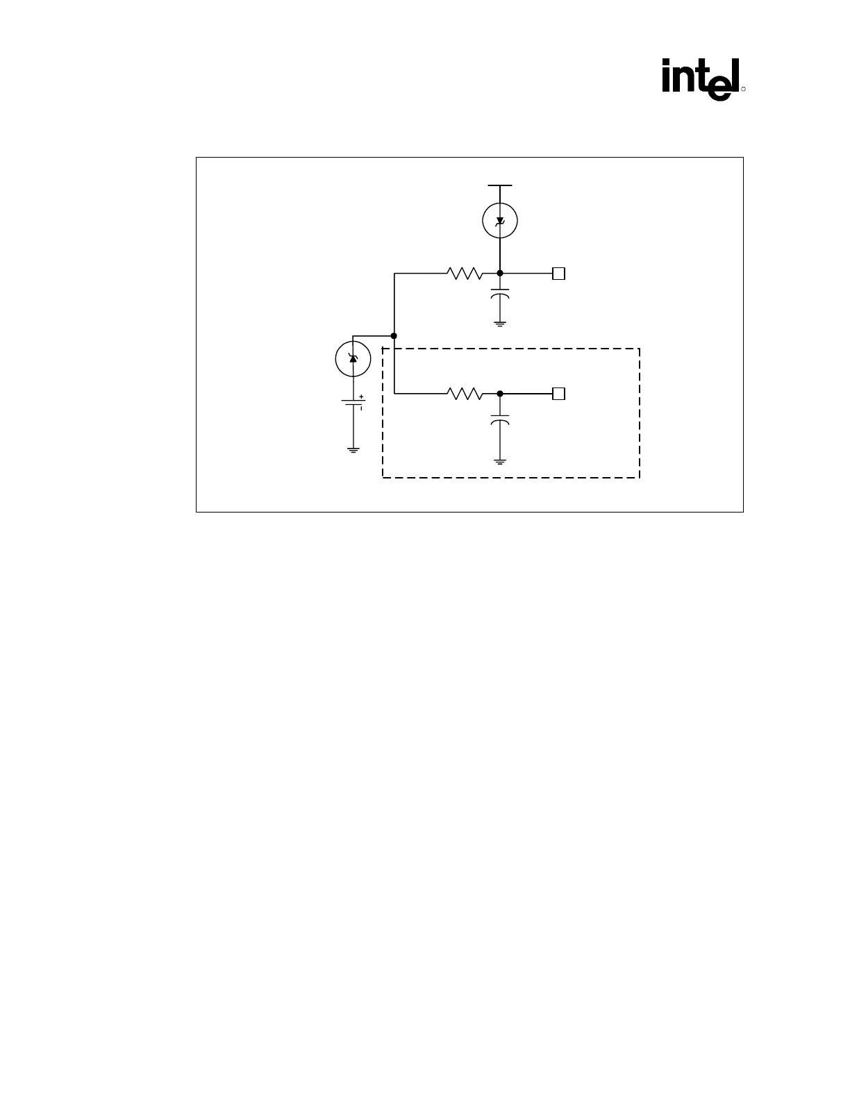
Figure 115. RTCRST External Circuit for the Intel
®
ICH2 RTC
VCC3_3SBY
Vcc RTC
1.0 µF
1 k
Ω
2.2 µF
8.2 k
Ω
RTCRST#
RTCRST
circuit
Diode /
battery circuit
RTC_RTCRESET_ext_circ
9.8.6 RTC Routing Guidelines
• All RTC OSC signals (RTCX1, RTCX2, VBIAS) should all be routed with trace lengths of
less than 1 inch, the shorter the better.
• Minimize the capacitance between RTCX1 and RTCX2 in the routing (optimal would be a
ground line between them).
• Put a ground plane under all of the external RTC circuitry.
• Do not route any switching signals under the external components (unless on the other side of
the ground plane).
9.8.7 VBIAS DC Voltage and Noise Measurements
• Steady state VBIAS will be a DC voltage of about 0.38 V ±0.06 V
• VBIAS will be “kicked” when the battery is inserted to about 0.7–1.0 V, but it will come back
to its DC value within a few ms
• Noise on VBIAS must be kept to a minimum, 200 mV or less.
• VBIAS is very sensitive and cannot be directly probed, it can be probed through a 0.01 µF
capacitor.
• Excess noise on VBIAS can cause the ICH2 internal oscillator to misbehave or even stop
completely.
• To minimize noise of VBIAS It is necessary to implement the routing guidelines described
above and the required external RTC circuitry as described in the Intel
®
82801BA I/O
Controller Hub 2 (ICH2) and Intel
®
82801BAM I/O Controller Hub 2 Mobile (ICH2-M)
Datasheet.