System Bus Routing
R
Intel
®
Pentium
®
4 Processor / Intel
®
850 Chipset Family Platform Design Guide 81
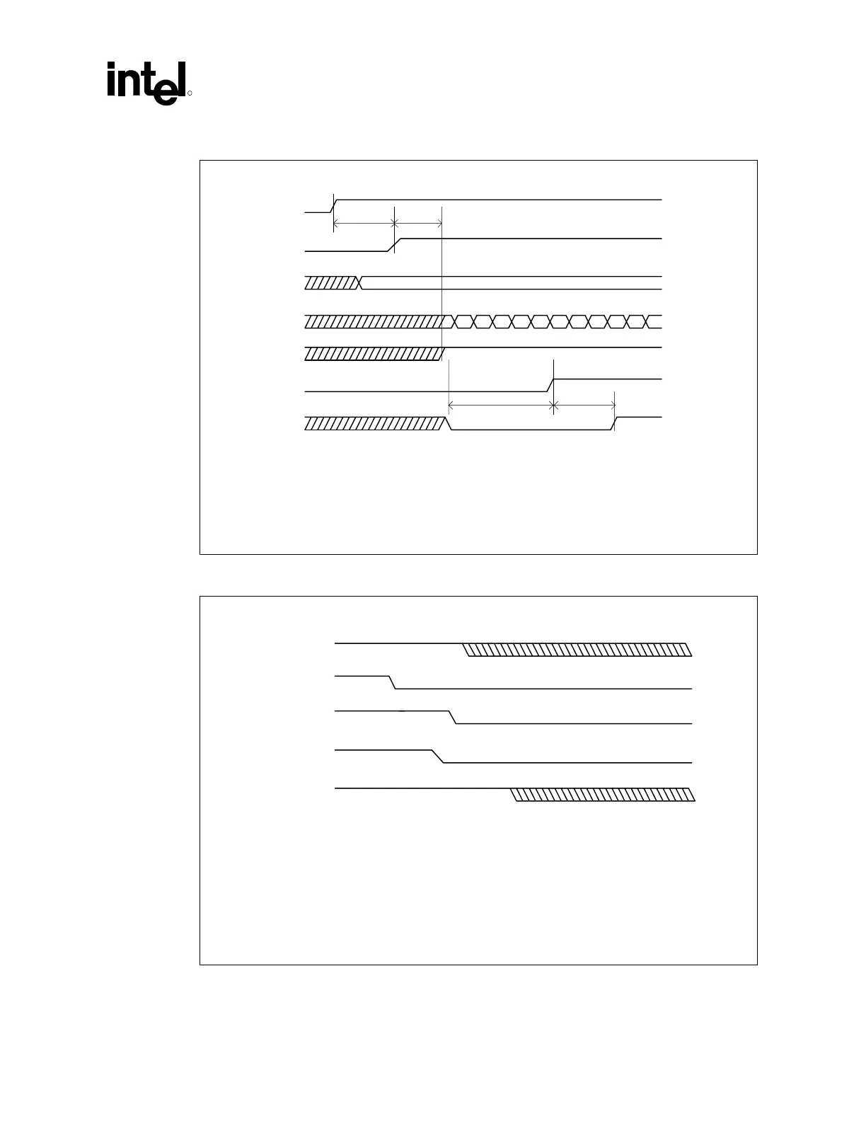
Figure 46: Power-on Sequence Timing Diagram
BCLK
VCC_CPU
PWRGOOD
RESET#
VCCVID
VID_GOOD
VID[4:0]
Tc Td
Ta= 1ms minimum (VCCVID > 1V to VID_GOOD high)
Tb= 50ms maximum (VID_GOOD to Vcc valid maximum time)
Tc= T37 (PWRGOOD inactive pulse width) = 10 BCLKs min
Td= T36 (PWRGOOD to RESET# de-assertion time) = 1ms(min), 10ms(max)
Note: VID_GOOD is not a processor signal. This signal is routed to the
output enable pin of the voltage regluator control silicon.
Power Up Sequence
Ta Tb
Power-on_Sequence_Timing
Figure 47. Power-off Sequence Timing Diagram
Power Down Sequence
Note: VID_GOOD is not a processor signal. This signal is routed to the
output enable pin of the voltage regluator control silicon.
1. This timing diagram is not intended to show specific times. Instead a
general ordering of events with respect to time should be observed.
2. When VCCVID is less than 1V, VID_GOOD must be low.
3. Vcc must be disabled before VID[4:0] becomes invalid.
VCC_CPU
PWRGOOD
VCCVID
VID_GOOD
VID[4:0]
Power-off_Sequence_Timing