Platform Clock Routing Guidelines
R
44 Intel
®
Pentium
®
4 Processor / Intel
®
850 Chipset Family Platform Design Guide
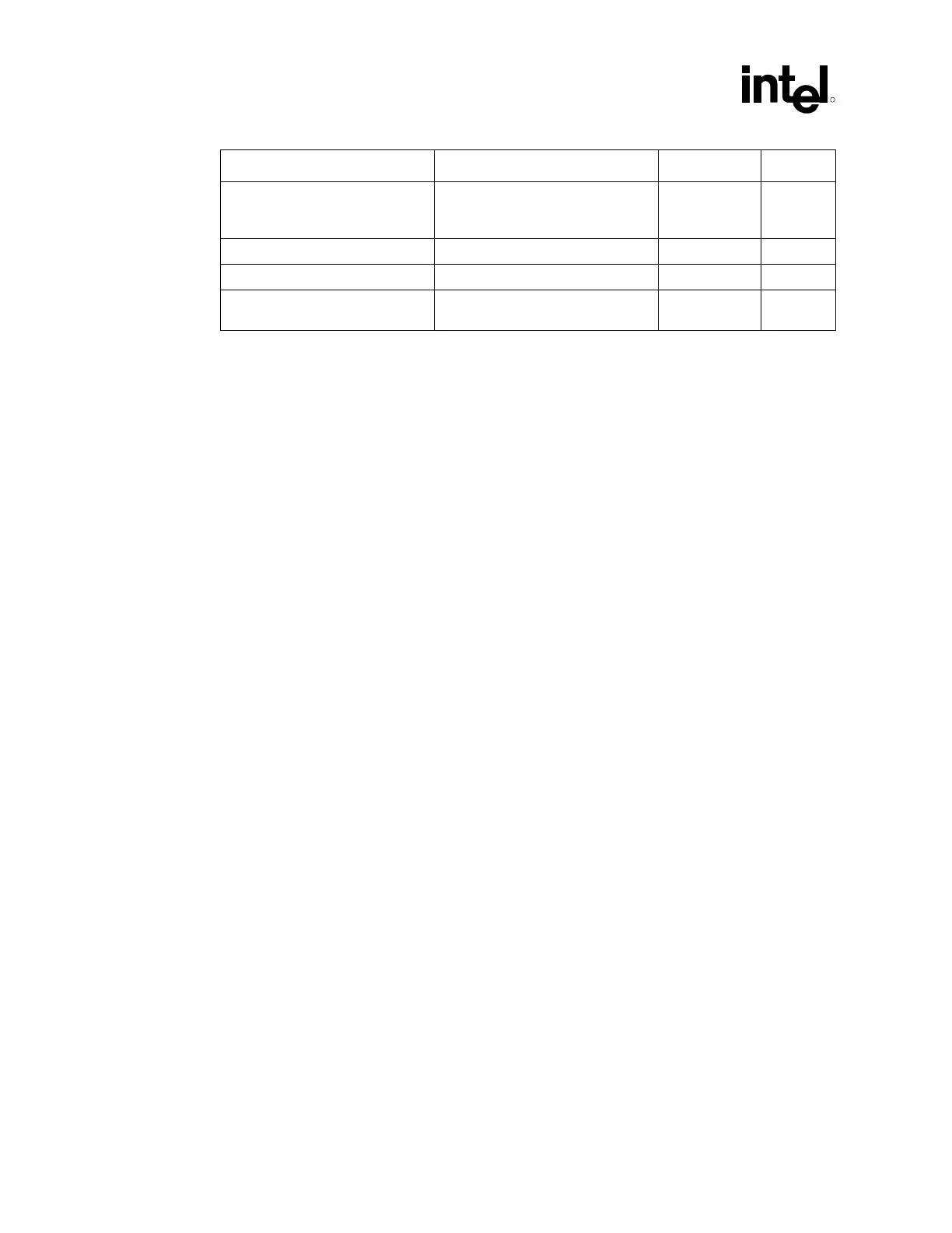
Layout Guideline Value Illustration Notes
Clock driver to processor and
clock driver to Chipset length
matching (LT)
0.600 inches ±0.010 inches (Add to
MCH trace length)
Figure 12 10
BCLK0 – BCLK1 length matching ±10 mils Figure 12 —
Rs Series termination value 33 Ω ±5% Figure 12 —
Rt Shunt termination value 49.9 Ω ±1% (for 50 Ω MB
impedance)
Figure 12 11
NOTES:
1. The skew budget includes clock driver output pair to output pair jitter (differential jitter), and skew, clock
skew due to interconnect process variation, and static skew due to layout differences between clocks to
all bus agents.
2. This number does not include clock driver common mode (cycle to cycle) jitter or spread spectrum
clocking.
3. The interconnect portion of the total budget for this specification assumes clock pairs are routed on
multiple routing layers and routed no longer than the maximum recommended lengths.
4. Skew measured at the load between any two bus agents. Measured at the crossing point.
5. Edge to edge spacing between the two traces of any differential pair. Uniform spacing should be
maintained along the entire length of the trace.
6. Clock traces are routed in a differential configuration. Maintain the minimum recommended spacing
between the two traces of the pair. Do not exceed the maximum trace spacing, as this will degrade the
noise rejection of the network.
7. Set line width to meet correct system board impedance. The line width value provided here is a
recommendation to meet the proper trace impedance based on the recommended stack-up.
8. The differential impedance of each clock pair is approximately 2*Zsingle-ended*(1-2*Kb) where Kb is
the backwards cross-talk coefficient. For the recommended trace spacing, Kb is very small and the
effective differential impedance is approximately equal to 2 times the single-ended impedance of each
half of the pair.
9. The single ended impedance of both halves of a differential pair should be targeted to be of equal value.
They should have the same physical construction. If the BCLK traces vary within the tolerances
specified, both traces of a differential pair must vary equally.
10. Length compensation for the processor socket and package delay is added to chipset routing to match
electrical lengths between the chipset and the processor from the die pad of each. Therefore, the
system board trace length for the chipset will be longer than that for the processor. Details of this
additional length will be included in a future revision of the processor package files.
11. Rt shunt termination value should match the system board impedance.
12. Minimize L1, L2 and L3 lengths. Long lengths on L2 and L3 degrade effectiveness of source termination
and contribute to ring back.