GR712RC-UM, Jun 2017, Version 2.9 30 www.cobham.com/gaisler
GR712RC
Which peripheral function that drives a shared I/O pin is determined through a set of enabling condi-
tions. Peripheral functions that are clock gated use the clock enable bit as I/O matrix select signal.
Enabling conditions for peripherals without clock gating are defined in table 9.
The peripherals are connected to the switch matrix I/O pin through a priority structure that makes sure
only one peripheral is granted the pin at a time. If no device is enabled, the pin defaults to the respec-
tive GPIO[63:0]. Note that there are two GRGPIO cores each with 32 bits, thus only 64 of the 67 pins
have a GPIO pin alternative. The first GRGPIO core is mapped on GPIO[31:0], and the second GPIO
core is mapped on GPIO[63:32]. Also note that when the CAN core is enabled, the output of pins 172,
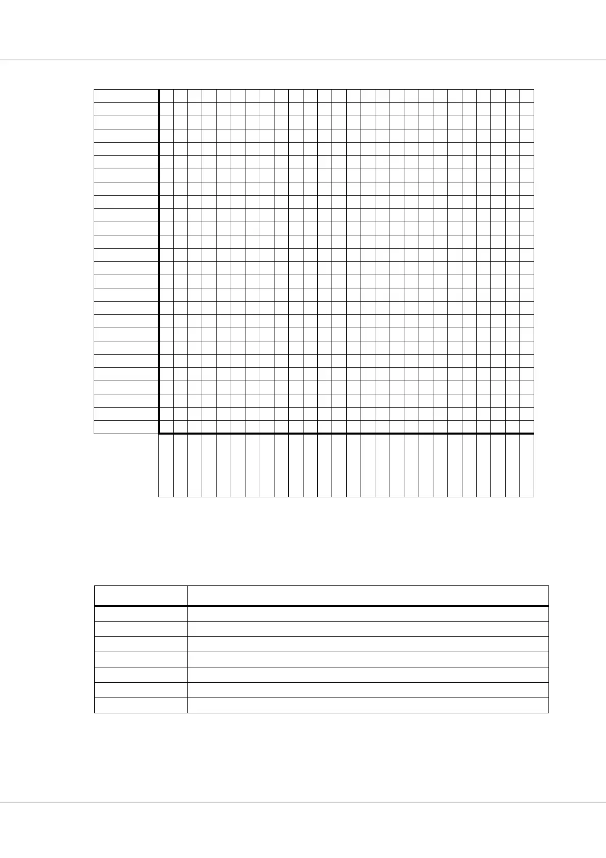
Table 8. Conflicting interfaces in the I/O switch matrix are marked with an X, with duplicates shown in bold typeface.
SDRAM (with RS) - XX
UART 0 -
UART 1 -
UART 2 -
UART 3 -
UART 4 - X
UART 5 - XX
SpaceWire 0 -
SpaceWire 1 -
SpaceWire 2 - XX
SpaceWire 3 - X
SpaceWire 4 X - XX
SpaceWire 5 X - XX
Ethernet - XX XX
CAN X X -
MIL-STD-1553B X - XXX
I2C - X
SPI - XX
SLINK X X - X
ASCS XXX-X
CCSDS TC 0 X X X X -
CCSDS TC 1 X X X-
CCSDS TC 2 X X-
CCSDS TC 3 XX -
CCSDS TC 4 X-
CCSDS TM X X -
SDRAM (with RS)
UART 0
UART 1
UART 2
UART 3
UART 4
UART 5
SpaceWire 0
SpaceWire 1
SpaceWire 2
SpaceWire 3
SpaceWire 4
SpaceWire 5
Ethernet
CAN
MIL-STD-1553B
I2C
SPI
SLINK
ASCS
CCSDS TC 0
CCSDS TC 1
CCSDS TC 2
CCSDS TC 3
CCSDS TC 4
CCSDS TM
TABLE 9. I/O switch matrix enables for non-gated devices
Device Enable
UART TX enable bit in APBUART control register
SPI Enable bit in SPICTRL control register
I2C Enable bit in I2CMST control register
ASCS Output enable bit in GRASCS control register
SLINK Enable bit in SLINKMST control register
SDRAM SDRAM enable in MCFG2
RS checkbits Reed-Solomon enable in MCFG3