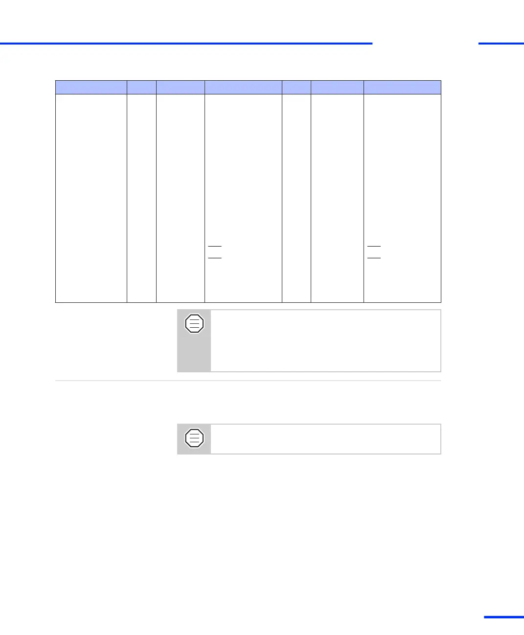
Connector (P2) Pin Sub-D Pin Signal Pin Sub-D Pin Signal
P2 65 P2B 28 SPWM1 P2 66 P2A 28 SPWM2
P2 67 P2B 12 SPWM3 P2 68 P2A 12 SPWM4
P2 69 P2B 45 SPWM5 P2 70 P2A 45 SPWM6
P2 71 P2B 29 SPWM7 P2 72 P2A 29 SPWM8
P2 73 P2B 13 SPWM9 P2 74 P2A 13 GND
P2 75 P2B 46 GND P2 76 P2A 46 GND
P2 77 P2B 30 SCAP1 P2 78 P2A 30 SCAP2
P2 79 P2B 14 SCAP3 P2 80 P2A 14 SCAP4
P2 81 P2B 47 GND P2 82 P2A 47 GND
P2 83 P2B 31 SXF P2 84 P2A 31 SBIO
P2 85 P2B 15 SSCLK P2 86 P2A 15 SSTE
P2 87 P2B 48 SSIMO P2 88 P2A 48 SSOMI
P2 89 P2B 32 GND P2 90 P2A 32 GND
P2 91 P2B 16 INT0 P2 92 P2A 16 INT1
P2 93 P2B 49 INT2 P2 94 P2A 49 INT3
P2 95 P2B 33 VCC1 (+ 5 V) P2 96 P2A 33 VCC1 (+ 5 V)
P2 97 P2B 17 VCC1 (+ 5 V) P2 98 P2A 17 VCC1 (+ 5 V)
P2 99 P2B 50 GND P2 100 P2A 50 GND
The DS1103 provides three VCC lines. The total load of
every VCC line (VCC1, VCC2, VCC3) must not exceed 500
mA.
For details on the VCC lines refer to Power Supply Outputs
on page 162.
Because the pin numbering used for Sub-D connectors is not
standardized, the following illustrations show the numbering scheme
used (viewed from the top of a female connector)
Do not rely on the numbers written on Sub-D
connectors.
Pinout of Sub‑D connectors
s
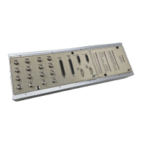
DS1103 Components
t
DS1103 Hardware Installation and Configuration November 2014
115
t