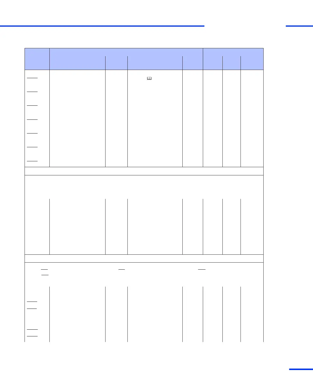
Signal Channel/Bit Numbers of Related RTI Blocks/RTLib Functions I/O Pin on …
Related RTI Block(s) Ch/Bit
(RTI)
Related RTLib Functions Ch/Bit
(RTLib)
DS1103 Sub‑D
Conn.
CP/CLP
IDX(1) DS1103ENC_SW_INDEX_Cx/
DS1103ENC_HW_INDEX_Cx
Ch 1 See Incremental Encoder
Interface ( DS1103 RTLib
Reference)
Ch 1 P3 49 P3B 9 CP32 6
IDX(1) P3 50 P3A 9 CP32 7
IDX(2) Ch 2 Ch 2 P3 57 P3B 43 CP33 6
IDX(2) P3 58 P3A 43 CP33 7
IDX(3) Ch 3 Ch 3 P3 65 P3B 28 CP34 6
IDX(3) P3 66 P3A 28 CP34 7
IDX(4) Ch 4 Ch 4 P3 73 P3B 13 CP35 6
IDX(4) P3 74 P3A 13 CP35 7
IDX(5) Ch 5 Ch 5 P3 81 P3B 47 CP36 6
IDX(5) P3 82 P3A 47 CP36 7
IDX(6) Ch 6 Ch 6 P3 41 P3B 24 CP37 6
IDX(6) P3 42 P3A 24 CP37 7
IDX(7) Ch 7 Ch 7 P3 33 P3B 39 CP39 6
IDX(7) P3 34 P3A 39 CP39 7
Serial Interface (RS232 mode)
n RS232 voltage range
n DCD (data carrier detect), CTS (clear to send), RTS (ready to send), DSR (data set ready), DTR (data terminal ready), RI (ring
indicator), RXD (receive), TXD (transmit)
n I/O circuit and further electrical characteristics: see Serial Interface on page 187
DCD * DS1103SER_SETUP/
DS1103SER_STAT/
DS1103SER_TX/
DS1103SER_RX/
DS1103SER_INT_Iy/
DS1103SER_INT_REC_LEV
P3 6 P3A 18 CP40 1
CTS * P3 9 P3B 35 CP40 8
RTS * P3 7 P3B 2 CP40 7
DSR * P3 10 P3A 35 CP40 6
DTR * P3 8 P3A 2 CP40 4
RI * P3 11 P3B 19 CP40 9
RXD * P3 5 P3B 18 CP40 2
TXD * P3 3 P3B 34 CP40 3
Serial Interface (RS422 mode)
n RS422 voltage range
n CTS, CTS (clear to send and inverted signal), RTS, RTS (ready to send and inverted signal), RXD, RXD (receive and inverted signal),
TXD, TXD (transmit and inverted signal)
n I/O circuit and further electrical characteristics: see Serial Interface on page 187
CTS * DS1103SER_SETUP/
DS1103SER_STAT/
DS1103SER_TX/
DS1103SER_RX/
DS1103SER_INT_Iy/
DS1103SER_INT_REC_LEV
P3 9 P3B 35 CP42 8
RTS * P3 7 P3B 2 CP42 7
CTS * P3 10 P3A 35 CP42 9
RTS * P3 8 P3A 2 CP42 6
RXD * P3 5 P3B 18 CP42 3
TXD * P3 3 P3B 34 CP42 2
RXD * P3 6 P3A 18 CP42 4
TXD * P3 4 P3A 34 CP42 1
s
Signal Mapping to I/O Pins
t
DS1103 Hardware Installation and Configuration November 2014
145
t