420
14.4.3 Input Sampling Time and A/D Conversion Time
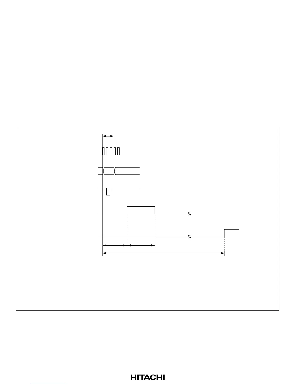
With a built-in sample-and-hold circuit, the A/D converter performs input sampling at time t
D
after control/status register (ADSCR) access is started. See figure 14.5 for A/D conversion timing
and table 14.4 for A/D conversion times.
The total conversion time includes t
D
and the input sampling time, as shown in figure 14.5. The
purpose of t
D
is to synchronize the ADCSR write time with the A/D conversion process; therefore
the duration of t
D
is variable. As a result, the total conversion time varies within the ranges shown
in table 14.4.
In scan mode, the ranges given in table 14.4 apply to the first conversion. The duration of the
second and subsequent conversion processes is fixed at 256 states (CKS = 0) or 128 states (CKS =
1).
CK
Write
signal
ADF
*1
Input sampling
timing
Address
*2
t
D
t
SPL
t
CONV
t
D
A/D start delay
t
SPL
Input sampling time
t
CONV
A/D conversion time
Notes: *1 ADSCR write cycle
*2 ADSCR address
Figure 14.5 A/D Conversion Timing

 Loading...
