550
(8) Serial Communication Interface Timing
Table 20.25 Serial Communication Interface Timing
Conditions: V
CC
= 3.3 V ±0.3V, AV
CC
= 3.3 V ±0.3V, AV
CC
= V
CC
±0.3V, AV
ref
= 3.0 V to
AV
CC
, V
SS
= AV
SS
= 0 V, φ = 12.5 to 20 MHz
*
1
, Ta = –20 to +75°C
*
2
Notes: *1 ROMless products only for 20 MHz version
*2 Regular-specification products; for wide-temperature-range products, Ta = –40 to
+85°C
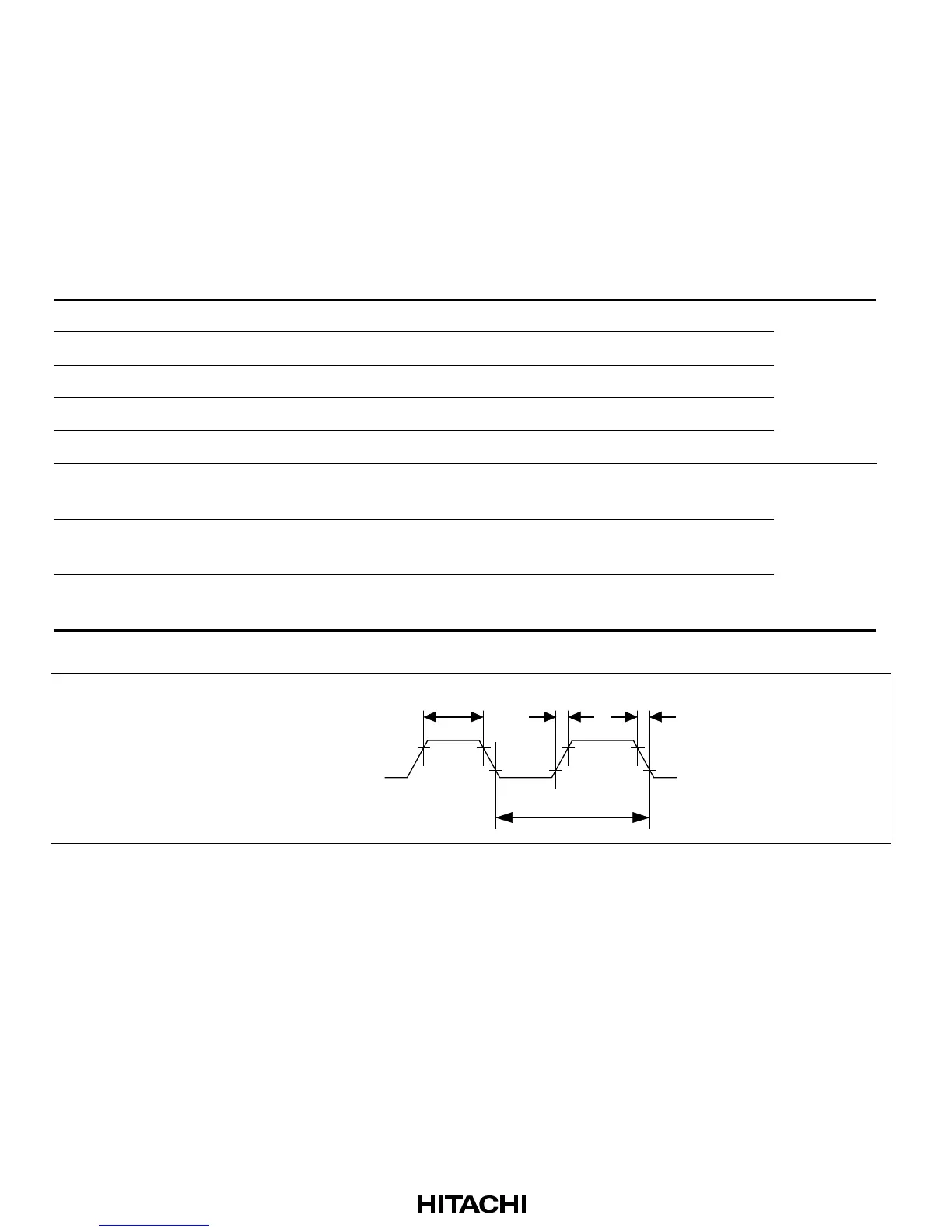
Item Symbol Min Max Unit Figure
Input clock cycle t
scyc
4—t
cyc
20.71
Input clock cycle (synchronous mode) t
scyc
6—t
cyc
Input clock pulse width t
SCKW
0.4 0.6 t
scyc
Input clock rise time t
SCKr
— 1.5 t
cyc
Input clock fall time t
SCKf
— 1.5 t
cyc
Transmit data delay time (synchronous
mode)
t
TXD
— 100 ns 20.72
Receive data setup time (synchronous
mode)
t
RXS
100 — ns
Receive data hold time (synchronous
mode)
t
RXH
100 — ns
SCK0, SCK1
t
scyc
t
SCKW
t
SCKr
t
SCKf
Figure 20.71 Input Clock Timing

 Loading...
