608
Table A.42 Bit Functions (cont)
Description
Bit Bit Name Value
DRAM Space
(BCRDRAME = 1)
Area 1 External Memory Space
(BCRDRAME = 1)
1 Write wait
state control
0 Column address cycle: 1 cycle
(short-pitch)
Setting prohibited
(WW1)
1 Column address cycle: Wait state
is 2 cycles + WAIT (long-pitch)
(Initial value)
Wait state is 2 cycles + WAIT
Note: *During a CBR refresh, the WAIT signal is ignored and the wait state inserted using the
RLW1 and RLW0 bits.
A.2.42 Wait State Control Register 2 (WCR2) BSC
• Start Address: H'5FFFFA4
• Bus Width: 8/16/32
Register Overview:
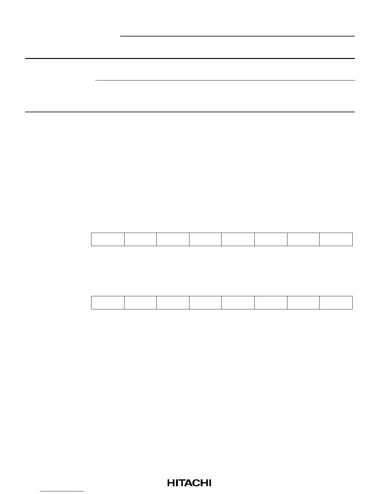
Bit: 15 14 13 12 11 10 9 8
Bit name: DRW7 DRW6 DRW5 DRW4 DRW3 DRW2 DRW1 DRW0
Initial value: 1 1 1 1 1 1 1 1
R/W: R/W R/W R/W R/W R/W R/W R/W R/W
Bit: 7 6 5 4 3 2 1 0
Bit name: DWW7 DWW6 DWW5 DWW4 DWW3 DWW2 DWW1 DWW0
Initial value: 1 1 1 1 1 1 1 1
R/W: R/W R/W R/W R/W R/W R/W R/W R/W