578
A.2.14 Timer Control Registers 0–4 (TCR0–TCR4) ITU
• Start Address: H'5FFFF04 (channel 0), H'5FFFF0E (channel 1), H'5FFFF18 (channel 2),
H'5FFFF22 (channel 3), H'5FFFF32 (channel 4)
• Bus Width: 8
Register Overview:
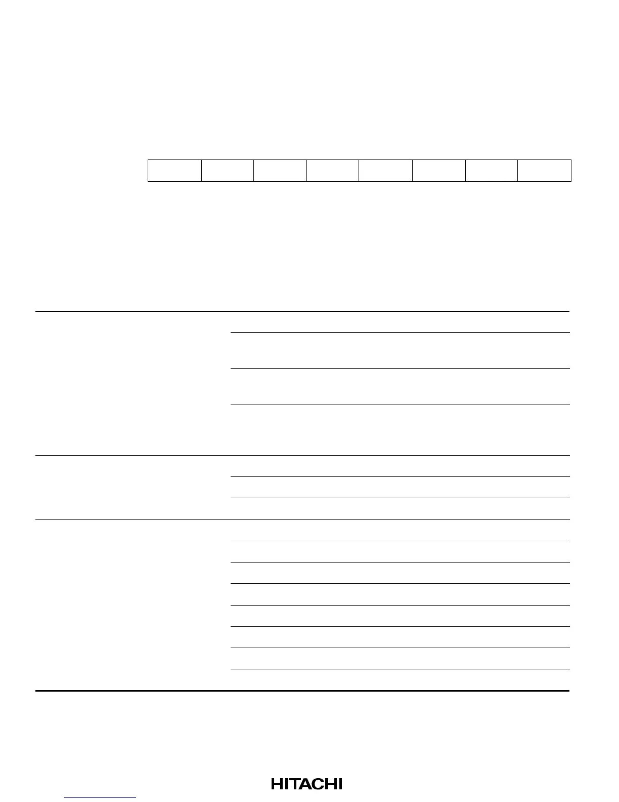
Bit: 7 6 5 4 3 2 1 0
Bit name: — CCLR1 CCLR0 CKEG1 CKEG0 TPSC2 TPSC1 TPSC0
Initial value: * 0000000
R/W: — R/W R/W R/W R/W R/W R/W R/W
Note: *Undetermined
Table A.15 TCR0–TCR4 Bit Functions
Bit Bit name Value Description
6,5 Counter clear 1, 0 (CCLR1, 0 0 TCNT clear disabled (Initial value)
CCLR0)
0 1 TCNT cleared upon GRA compare match/input
capture
1 0 TCNT cleared upon GRB compare match/input
capture
1 1 Synchronized clear. TCNT cleared in
synchronization with counter clear of other timers
operating in sync
4,3 Clock edge 1, 0 (CKEG1, 0 0 Count on rising edge (Initial value)
CKEG0)
0 1 Count on falling edge
1 * Count on both rising and falling edges
2–0 Timer prescaler 2–0 0 0 0 Internal clock: Count on φ (Initial value)
(TPSC2–TPSC0)
0 0 1 Internal clock: Count on φ/2
0 1 0 Internal clock: Count on φ/4
0 1 1 Internal clock: Count on φ/8
1 0 0 External clock A: Count on TCLKA pin input
1 0 1 External clock B: Count on TCLKB pin input
1 1 0 External clock C: Count on TCLKC pin input
1 1 1 External clock D: Count on TCLKD pin input
Note: *0 or 1
 Loading...

