EDN S
EPTEMBER
24, 1998
b 119
ARM designs mP cores and cached macrocells for its licensees.
Partners offering ASICs with embedded ARM cores are
Atmel/ES2, Cirrus Logic, Mitel, IBM, LG Semicon (www.
lgsemicon.co.kr/), LSI Logic, Lucent (www.lucent.com),
National Semiconductor, NEC, Oki, Samsung, Seiko Epson
(www.epson.co.jp/), Sharp, Symbios Logic (www.symbios.
com), TI, and VLSI. Some partners offer the ARM core in
embedded products for vertical markets.
ARM processors comprise the ARM7 Thumb, ARM9
Thumb, and StrongARM product families. (ARM will
announce ARM10 in October.) All the processors support the
ARM instruction set, providing full software compatibility
over a range of performance and cost.
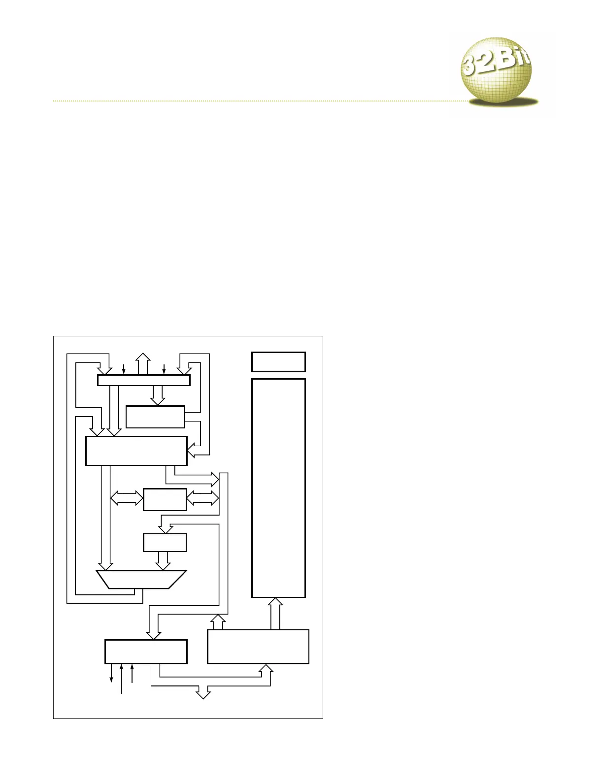
The ARM cores and cached macrocells implement a
load/store architecture and have 31 general-purpose registers
with 16 simultaneously visible. A fast interrupt has a mini-
mum latency of four processor cycles and uses seven private
registers to minimize state-saving overhead. All registers,
excluding the program counter, are general-purpose,
although a set of conventions, the ARM Procedure Call Stan-
dard, governs the registers’ use for C compatibility.
The ARM cores and cached macrocells support user and
supervisor modes for controlling access; they handle inter-
rupt-request, fast-interrupt-request, abort, and undefined
exception-processing modes. Modes use register windows to
overlay some of the 16 general-purpose registers.
The Thumb architectural extension is primarily a 16-bit
subset of the 32-bit instruction set. On execution, the
Thumb module, residing within the instruction pipeline,
decompresses the 16-bit instructions back to 32-bit instruc-
tions without added delay. The Thumb module adds about
6% to the core’s die size but helps increase code density and
overcome the waste from using 32-bit fixed-length instruc-
tions.
The bus clock for most ARM cached macrocells can be syn
-
chronous or asynchronous with respect to the internal cache
clock. All ARM cached macrocells contain a write buffer,
which lets execution continue while writes are pending. The
buffer holds 8 words at four independent addresses.
The ARM7 Thumb family comprises the ARM7TDMI core
and ARM7x0T cached macrocells. This architecture, Version
4T, consists of a three-stage—fetch, decode, and execute—
pipeline to achieve single-cycle instruction execution.
All cores use an 8-bit Booth multiplier, which executes
in five or fewer cycles for 32332-bit multiply and
offers 64-bit multiplication. The ARM740T integrates
a simplified memory-management unit (MMU) that
allows you to specify eight memory areas by individ-
ually programming their base address, size, cache con-
trol, write-buffer control, and access permissions. This
approach simplifies the programmer model and
reduces the core size to less than that of the ARM710T
and ARM720T.
ARM based the ARM9 Thumb family, available as
the ARM940T, on the ARM9TDMI core. The core is
also an implementation of the ARM Version 4T archi-
tecture but with a five-stage—fetch, decode, execute,
memory, and write-back—pipeline. The additional
pipeline depth and design implementation double the
performance over the ARM7 Thumb cores. The bus
architecture also differs, using a Har
vard approach
compared with the ARM7 Thumb core’s von Neu-
mann architecture. The ARM940T implements the
same MMU as the ARM740T
. You can use the cache in
write-through and -back modes; write-back mode
reduces the number of external transactions from the
core.
StrongARM uses a five-stage pipeline and Harvard
ar
chitecture and supports Version 4 of the ARM ar
chi-
tecture. It provides a fourfold increase in performance
over the ARM7 Thumb cores. Intel now produces and
develops StrongARM, which is available as the stan
-
dard SA-110 processor and as part of custom logic
products.
The cores avoid excess pipeline flushes—Strong-
ARM by using early branch execution and ARM7 by
using static branch prediction, always taking the rear
branch as in a loop. The SA-110 has separate instruc
-
tion and data MMUs. The translation-look-aside
buffers (TLBs) have 32 entries that can each map a seg
-
ment, large page, or small page and use a round-robin
replacement algorithm. The data TLB supports both