XA User Guide 2-19 3/24/97
Second, the number of address lines may be configured in order to make optimal use of I/O
ports. Since external bus functions are typically shared with I/O ports and/or peripheral I/O
functions, it is advantageous to set the number of address lines to only what is needed for a
particular application, freeing I/O pins for other uses.
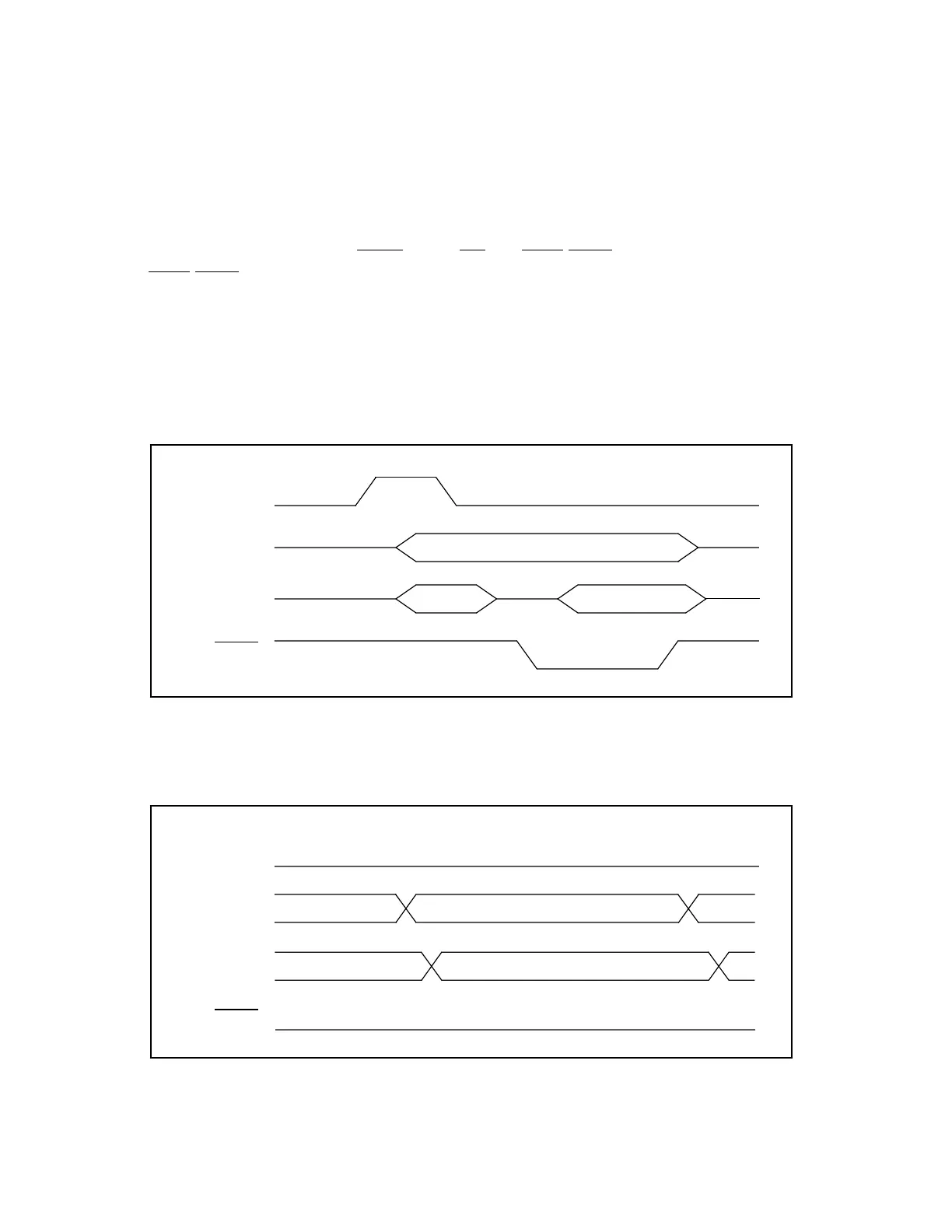
2.6.3 Bus Timing
The standard XA bus also provides a high degree of bus timing configurability. There are
separate controls for ALE width,
PSEN width, RD and WRL/WRH width, and data hold time
from
WRL/WRH. These times are programmable in a range that will support most RAMs,
ROMs, EPROMs, and peripheral devices over a wide range of oscillator frequencies without the
need for additional external latches, buffers, or WAIT state generators.
The following figures show the basic sequence of events and timing of typical XA bus accesses.
For more detailed information, consult Section 7 and the device data sheet.
Figure 2.12 Typical External Code Read.
Figure 2.13 Optimized (Sequential Burst) External Code Read.
ALE
PSEN
Address bus
Data bus
address
instruction data
code address
ALE
PSEN
Address bus
Data bus
instruction data
instruction data
code address
code address