8254
231164–3
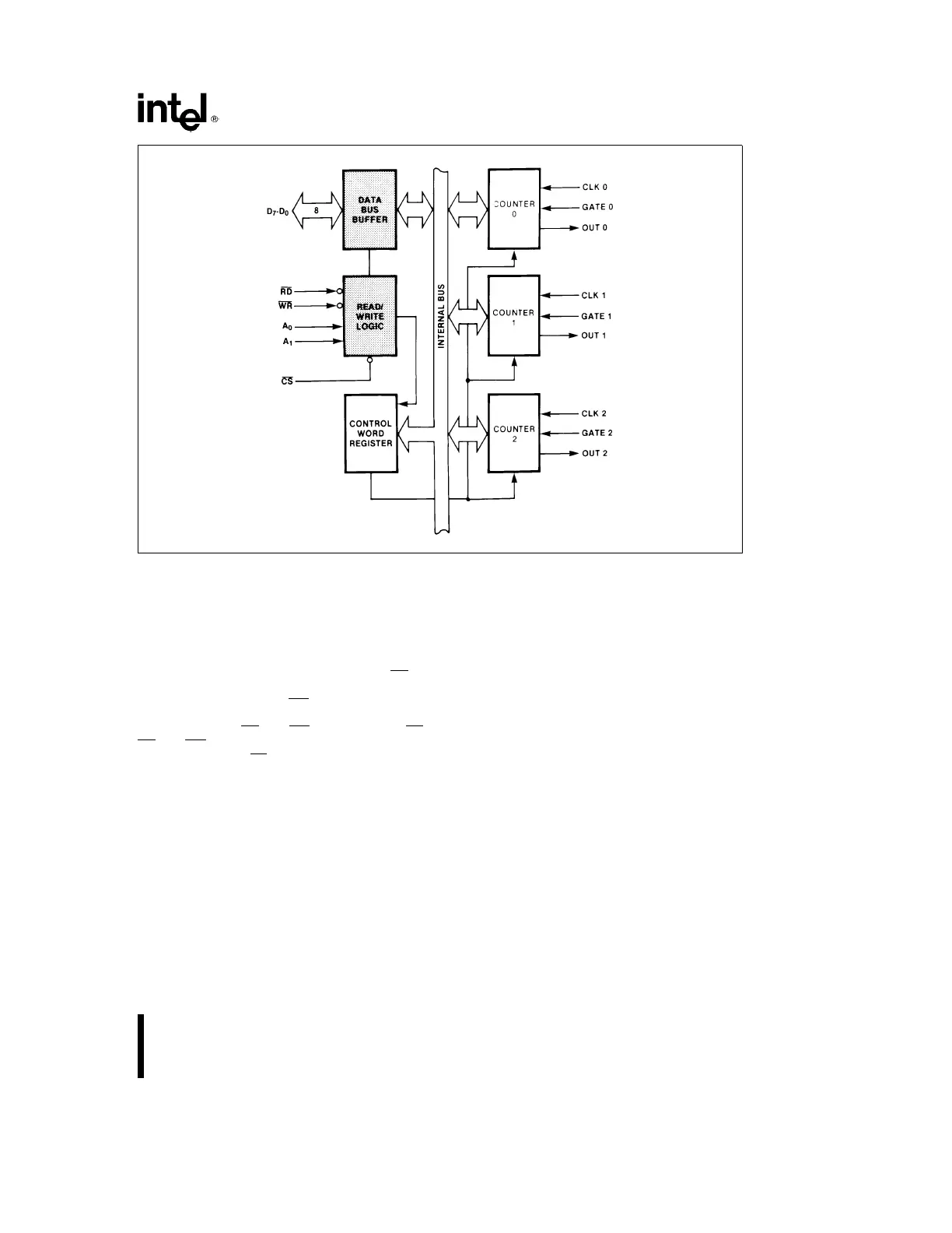
Figure 3. Block Diagram Showing Data Bus Buffer and Read/Write Logic Functions
READ/WRITE LOGIC
The Read/Write Logic accepts inputs from the sys-
tem bus and generates control signals for the other
functional blocks of the 8254. A
1
and A
0
select one
of the three counters or the Control Word Register
to be read from/written into. A ‘‘low’’ on the RD
in-
put tells the 8254 that the CPU is reading one of the
counters. A ‘‘low’’ on the WR
input tells the 8254
that the CPU is writing either a Control Word or an
initial count. Both RD
and WR are qualified by CS;
RD
and WR are ignored unless the 8254 has been
selected by holding CS
low.
CONTROL WORD REGISTER
The Control Word Register (see Figure 4) is selected
by the Read/Write Logic when A
1
,A
0
e
11. If the
CPU then does a write operation to the 8254, the
data is stored in the Control Word Register and is
interpreted as a Control Word used to define the
operation of the Counters.
The Control Word Register can only be written to;
status information is available with the Read-Back
Command.
COUNTER 0, COUNTER 1, COUNTER 2
These three functional blocks are identical in opera-
tion, so only a single Counter will be described. The
internal block diagram of a single counter is shown
in Figure 5.
The Counters are fully independent. Each Counter
may operate in a different Mode.
The Control Word Register is shown in the figure; it
is not part of the Counter itself, but its contents de-
termine how the Counter operates.
The status register, shown in Figure 5, when
latched, contains the current contents of the Control
Word Register and status of the output and null
count flag. (See detailed explanation of the Read-
Back command.)
The actual counter is labelled CE (for ‘‘Counting Ele-
ment’’). It is a 16-bit presettable synchronous down
counter.
OL
M
and OL
L
are two 8-bit latches. OL stands for
‘‘Output Latch’’; the subscripts M and L stand for
‘‘Most significant byte’’ and ‘‘Least significant byte’’
3