80C187
ELECTRICAL DATA
Absolute Maximum Ratings*
Case Temperature Under Bias (T
C
)ÀÀÀ0
§
Cto
a
85
§
C
Storage Temperature ÀÀÀÀÀÀÀÀÀÀ
b
65
§
Cto
a
150
§
C
Voltage on Any Pin
with Respect to GroundÀÀÀÀ
b
0.5V to V
CC
a
0.5V
Power DissipationÀÀÀÀÀÀÀÀÀÀÀÀÀÀÀÀÀÀÀÀÀÀÀÀÀÀ1.5W
Power and Frequency Requirements
The typical relationship between I
CC
and the fre-
quency of operation F is as follows:
I
CC
typ
e
55
a
5
*
F mA where F is in MHz.
When the frequency is reduced below the minimum
operating frequency specified in the AC Characteris-
tics table, the internal states of the 80C187 may be-
come indeterminate. The 80C187 clock cannot be
stopped; otherwise, I
CC
would increase significantly
beyond what the equation above indicates.
NOTICE: This is a production data sheet. The specifi-
cations are subject to change without notice.
*
WARNING: Stressing the device beyond the ‘‘Absolute
Maximum Ratings’’ may cause permanent damage.
These are stress ratings only. Operation beyond the
‘‘Operating Conditions’’ is not recommended and ex-
tended exposure beyond the ‘‘Operating Conditions’’
may affect device reliability.
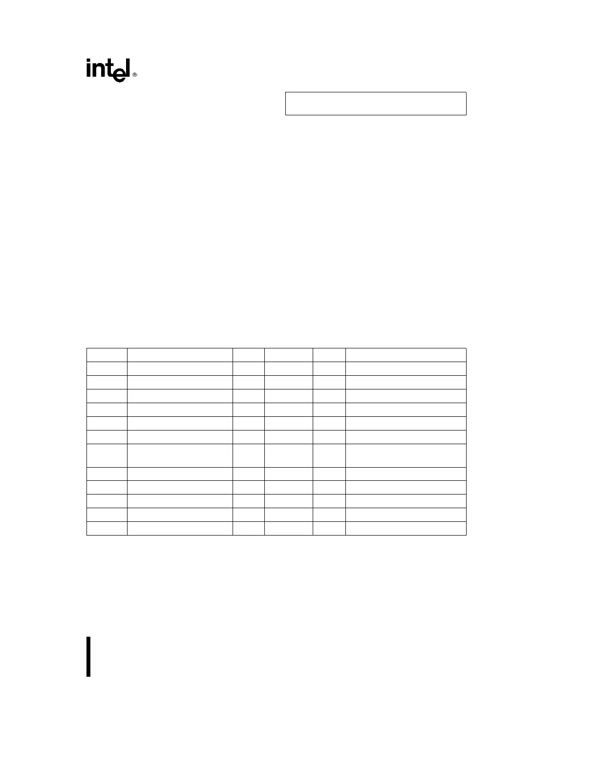
DC Characteristics T
C
e
0
§
Cto
a
85
§
C, V
CC
ea
5V
g
10%
Symbol Parameter Min Max Units Test Conditions
V
IL
Input LOW Voltage
b
0.5
a
0.8 V
V
IH
Input HIGH Voltage 2.0 V
CC
a
0.5 V
V
ICL
Clock Input LOW Voltage
b
0.5
a
0.8 V
V
ICH
Clock Input HIGH Voltage 2.0 V
CC
a
0.5 V
V
OL
Output LOW Voltage 0.45 V I
OL
e
3.0 mA
V
OH
Output HIGH Voltage 2.4 V I
OH
eb
0.4 mA
I
CC
Power Supply Current 156 mA 16 MHz
135 mA 12.5 MHz
I
LI
Input Leakage Current
g
10 mA0V
s
V
IN
s
V
CC
I
LO
I/O Leakage Current
g
10 mA 0.45V
s
V
OUT
s
V
CC
b
0.45V
C
IN
Input Capacitance 10 pF F
C
e
1 MHz
C
O
I/O or Output Capacitance 12 pF F
C
e
1 MHz
C
CLK
Clock Capacitance 20 pF F
C
e
1 MHz
21