8254
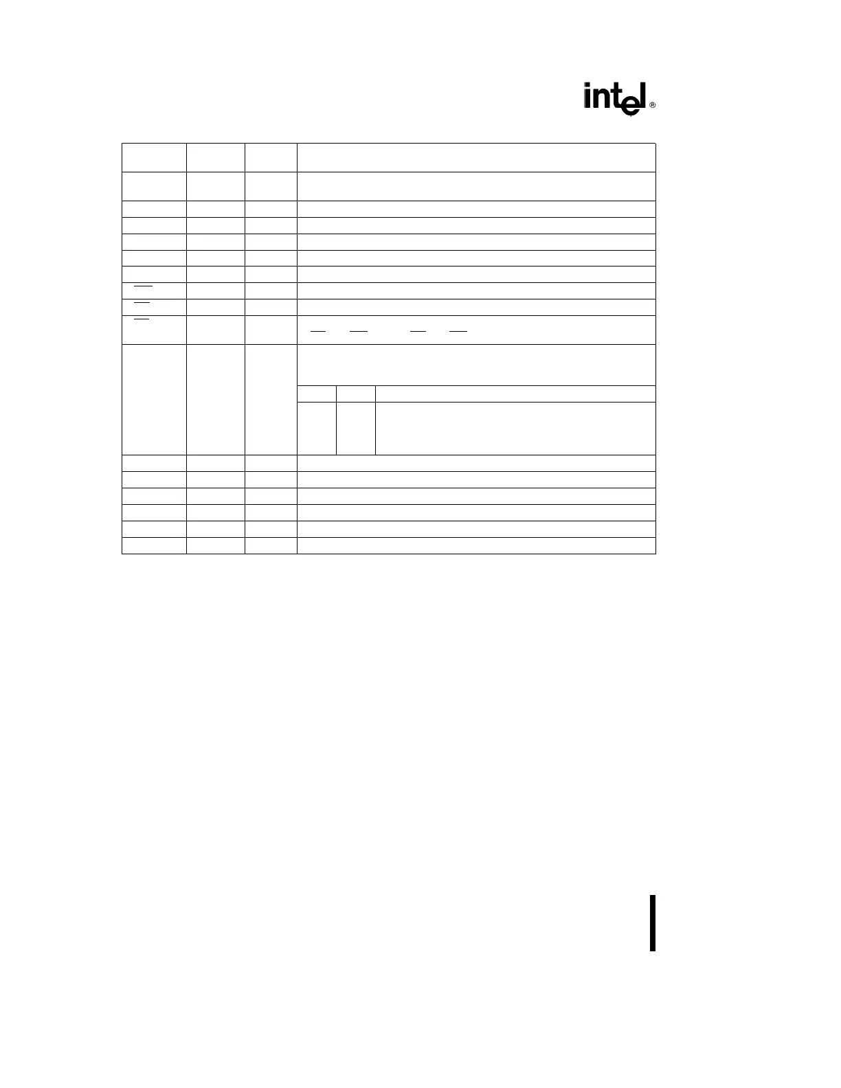
Table 1. Pin Description
Symbol
Pin
Type Name and Function
No.
D
7
–D
0
1–8 I/O DATA: Bi-directional three state data bus lines, connected to system
data bus.
CLK 0 9 I CLOCK 0: Clock input of Counter 0.
OUT 0 10 O OUTPUT 0: Output of Counter 0.
GATE 0 11 I GATE 0: Gate input of Counter 0.
GND 12 GROUND: Power supply connection.
V
CC
24 POWER:
a
5V power supply connection.
WR 23 I WRITE CONTROL: This input is low during CPU write operations.
RD 22 I READ CONTROL: This input is low during CPU read operations.
CS 21 I CHIP SELECT: A low on this input enables the 8254 to respond to
RD and WR signals. RD and WR are ignored otherwise.
A
1
,A
0
20–19 I ADDRESS: Used to select one of the three Counters or the Control
Word Register for read or write operations. Normally connected to
the system address bus.
A
1
A
0
Selects
0 0 Counter 0
0 1 Counter 1
1 0 Counter 2
1 1 Control Word Register
CLK 2 18 I CLOCK 2: Clock input of Counter 2.
OUT 2 17 O OUT 2: Output of Counter 2.
GATE 2 16 I GATE 2: Gate input of Counter 2.
CLK 1 15 I CLOCK 1: Clock input of Counter 1.
GATE 1 14 I GATE 1: Gate input of Counter 1.
OUT 1 13 O OUT 1: Output of Counter 1.
FUNCTIONAL DESCRIPTION
General
The 8254 is a programmable interval timer/counter
designed for use with Intel microcomputer systems.
It is a general purpose, multi-timing element that can
be treated as an array of I/O ports in the system
software.
The 8254 solves one of the most common problems
in any microcomputer system, the generation of ac-
curate time delays under software control. Instead of
setting up timing loops in software, the programmer
configures the 8254 to match his requirements and
programs one of the counters for the desired delay.
After the desired delay, the 8254 will interrupt the
CPU. Software overhead is minimal and variable
length delays can easily be accommodated.
Some of the other counter/timer functions common
to microcomputers which can be implemented with
the 8254 are:
#
Real time clock
#
Event-counter
#
Digital one-shot
#
Programmable rate generator
#
Square wave generator
#
Binary rate multiplier
#
Complex waveform generator
#
Complex motor controller
Block Diagram
DATA BUS BUFFER
This 3-state, bi-directional, 8-bit buffer is used to in-
terface the 8254 to the system bus (see Figure 3).
2