8254
ABSOLUTE MAXIMUM RATINGS*
Ambient Temperature Under Bias ÀÀÀÀÀÀ0
§
Cto70
§
C
Storage Temperature ÀÀÀÀÀÀÀÀÀÀ
b
65
§
Cto
a
150
§
C
Voltage on Any Pin with
Respect to GroundÀÀÀÀÀÀÀÀÀÀÀÀÀÀ
b
0.5V to
a
7V
Power Dissipation ÀÀÀÀÀÀÀÀÀÀÀÀÀÀÀÀÀÀÀÀÀÀÀÀÀÀÀ1W
NOTICE: This is a production data sheet. The specifi-
cations are subject to change without notice.
*
WARNING: Stressing the device beyond the ‘‘Absolute
Maximum Ratings’’ may cause permanent damage.
These are stress ratings only. Operation beyond the
‘‘Operating Conditions’’ is not recommended and ex-
tended exposure beyond the ‘‘Operating Conditions’’
may affect device reliability.
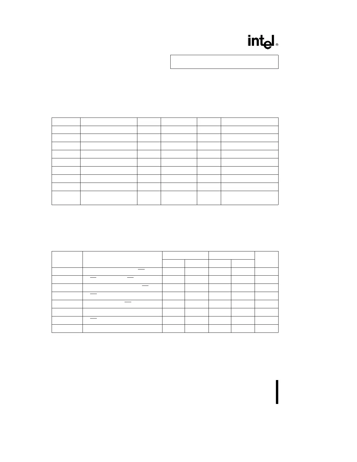
D.C. CHARACTERISTICS T
A
e
0
§
Cto70
§
C, V
CC
e
5V
g
10%
Symbol Parameter Min Max Units Test Conditions
V
IL
Input Low Voltage
b
0.5 0.8 V
V
IH
Input High Voltage 2.0 V
CC
a
0.5V V
V
OL
Output Low Voltage 0.45 V I
OL
e
2.0 mA
V
OH
Output High Voltage 2.4 V I
OH
eb
400 mA
I
IL
Input Load Current
g
10 mAV
IN
e
V
CC
to 0V
I
OFL
Output Float Leakage
g
10 mAV
OUT
e
V
CC
to 0.45V
I
CC
V
CC
Supply Current 170 mA
C
IN
Input Capacitance 10 pF f
c
e
1 MHz
C
I/0
I/O Capacitance 20 pF Unmeasured pins
returned to V
SS
(4)
A.C. CHARACTERISTICS T
A
e
0
§
Cto70
§
C, V
CC
e
5V
g
10%, GND
e
0V
Bus Parameters
(1)
READ CYCLE
Symbol Parameter
8254 8254-2
Unit
Min Max Min Max
t
AR
Address Stable Before RD
v
45 30 ns
t
SR
CS Stable Before RD
v
00ns
t
RA
Address Hold Time After RD
u
00ns
t
RR
RD Pulse Width 150 95 ns
t
RD
Data Delay from RD
v
120 85 ns
t
AD
Data Delay from Address 220 185 ns
t
DF
RD
u
to Data Floating 5 90 5 65 ns
t
RV
Command Recovery Time 200 165 ns
NOTE:
1. AC timings measured at V
OH
e
2.0V, V
OL
e
0.8V.
18