82C54
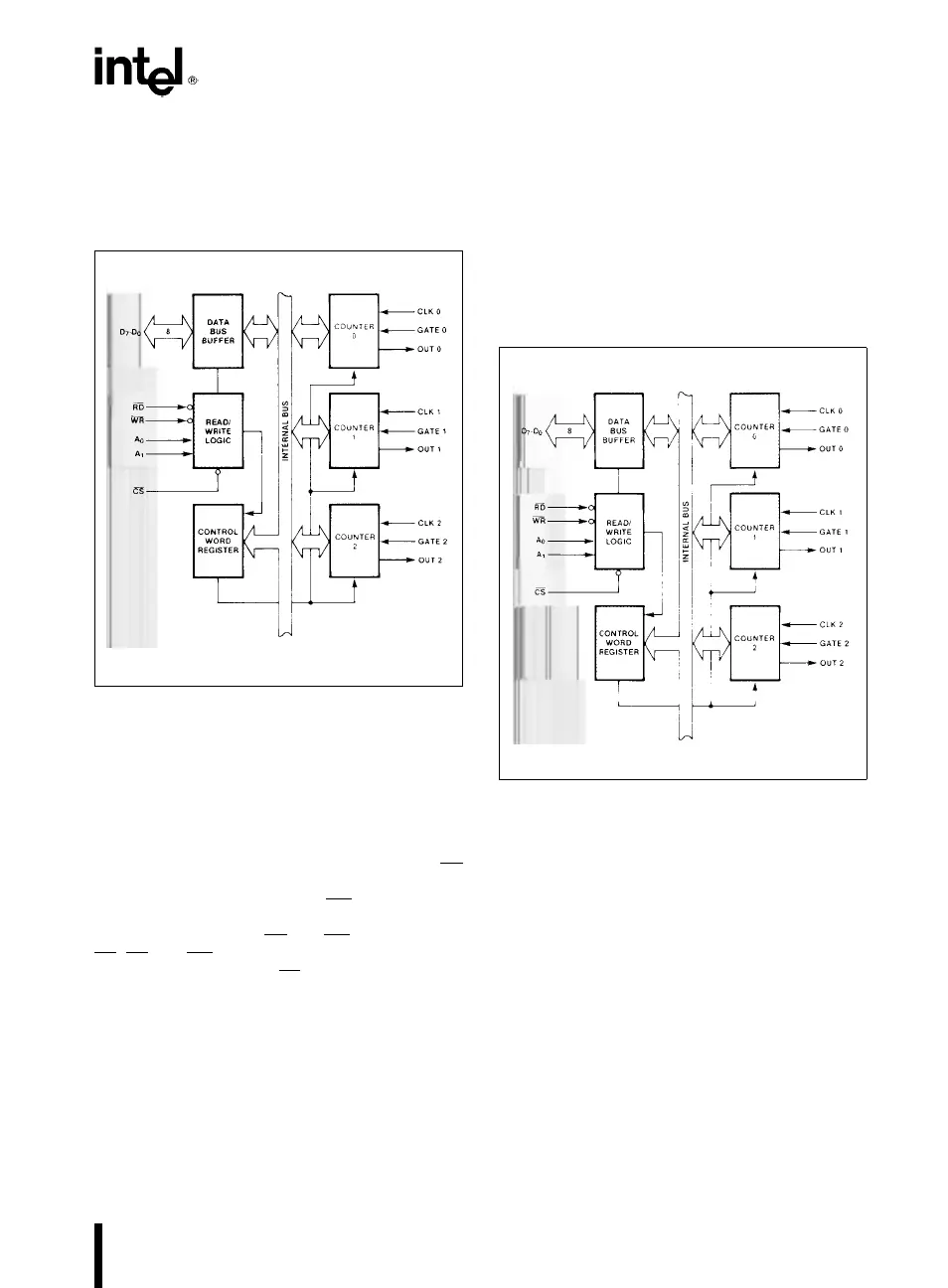
Block Diagram
DATA BUS BUFFER
This 3-state, bi-directional, 8-bit buffer is used to in-
terface the 82C54 to the system bus (see Figure 3).
231244–4
Figure 3. Block Diagram Showing Data Bus
Buffer and Read/Write Logic Functions
READ/WRITE LOGIC
The Read/Write Logic accepts inputs from the sys-
tem bus and generates control signals for the other
functional blocks of the 82C54. A
1
and A
0
select
one of the three counters or the Control Word Regis-
ter to be read from/written into. A ‘‘low’’ on the RD
input tells the 82C54 that the CPU is reading one of
the counters. A ‘‘low’’ on the WR
input tells the
82C54 that the CPU is writing either a Control Word
or an initial count. Both RD
and WR are qualified by
CS
;RDand WR are ignored unless the 82C54 has
been selected by holding CS
low.
The WR
Ý
and CLK signals should be synchronous.
This is accomplished by using a CLK input signal to
the 82C54 counters which is a derivative of the sys-
tem clock source. Another technique is to externally
synchronize the WR
Ý
and CLK input signals. This is
done by gating WR
Ý
with CLK.
CONTROL WORD REGISTER
The Control Word Register (see Figure 4) is selected
by the Read/Write Logic when A
1
,A
0
e
11. If the
CPU then does a write operation to the 82C54, the
data is stored in the Control Word Register and is
interpreted as a Control Word used to define the
operation of the Counters.
The Control Word Register can only be written to;
status information is available with the Read-Back
Command.
231244–5
Figure 4. Block Diagram Showing Control Word
Register and Counter Functions
COUNTER 0, COUNTER 1, COUNTER 2
These three functional blocks are identical in opera-
tion, so only a single Counter will be described. The
internal block diagram of a single counter is shown
in Figure 5.
The Counters are fully independent. Each Counter
may operate in a different Mode.
The Control Word Register is shown in the figure; it
is not part of the Counter itself, but its contents de-
termine how the Counter operates.
3