82C54
231244–6
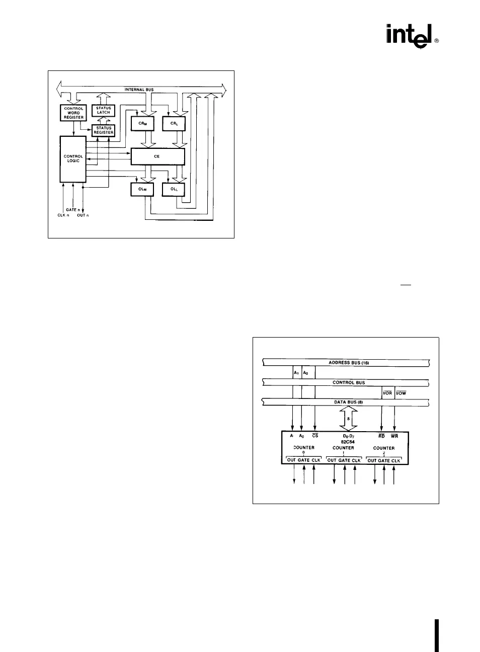
Figure 5. Internal Block Diagram of a Counter
The status register, shown in the Figure, when
latched, contains the current contents of the Control
Word Register and status of the output and null
count flag. (See detailed explanation of the Read-
Back command.)
The actual counter is labelled CE (for ‘‘Counting Ele-
ment’’). It is a 16-bit presettable synchronous down
counter.
OL
M
and OL
L
are two 8-bit latches. OL stands for
‘‘Output Latch’’; the subscripts M and L stand for
‘‘Most significant byte’’ and ‘‘Least significant byte’’
respectively. Both are normally referred to as one
unit and called just OL. These latches normally ‘‘fol-
low’’ the CE, but if a suitable Counter Latch Com-
mand is sent to the 82C54, the latches ‘‘latch’’ the
present count until read by the CPU and then return
to ‘‘following’’ the CE. One latch at a time is enabled
by the counter’s Control Logic to drive the internal
bus. This is how the 16-bit Counter communicates
over the 8-bit internal bus. Note that the CE itself
cannot be read; whenever you read the count, it is
the OL that is being read.
Similarly, there are two 8-bit registers called CR
M
and CR
L
(for ‘‘Count Register’’). Both are normally
referred to as one unit and called just CR. When a
new count is written to the Counter, the count is
stored in the CR and later transferred to the CE. The
Control Logic allows one register at a time to be
loaded from the internal bus. Both bytes are trans-
ferred to the CE simultaneously. CR
M
and CR
L
are
cleared when the Counter is programmed. In this
way, if the Counter has been programmed for one
byte counts (either most significant byte only or least
significant byte only) the other byte will be zero.
Note that the CE cannot be written into; whenever a
count is written, it is written into the CR.
The Control Logic is also shown in the diagram. CLK
n, GATE n, and OUT n are all connected to the out-
side world through the Control Logic.
82C54 SYSTEM INTERFACE
The 82C54 is treated by the systems software as an
array of peripheral I/O ports; three are counters and
the fourth is a control register for MODE program-
ming.
Basically, the select inputs A
0
,A
1
connect to the A
0
,
A
1
address bus signals of the CPU. The CS can be
derived directly from the address bus using a linear
select method. Or it can be connected to the output
of a decoder, such as an Intel 8205 for larger sys-
tems.
231244–7
Figure 6. 82C54 System Interface
4