Intel387
TM
SX MATH COPROCESSOR
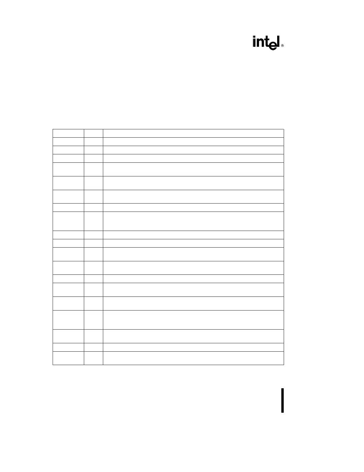
1.1 Pin Description Table
The following table lists a brief description of each
pin on the Intel387 SX Math CoProcessor. For a
more complete description refer to Section 4.1 Sig-
nal Description. The following definitions are used in
these descriptions:
Ý
The signal is active LOW.
I Input Signal
O Output Signal
I/O Input and Output Signal
Symbol Type Name and Function
ADS
Ý
I ADDRESS STROBE indicates that the address and bus cycle definition is valid.
BUSY
Ý
O BUSY indicates that the Math CoProcessor is currently executing an instruction.
CKM I CLOCKING MODE is used to select synchronous or asynchronous clock modes.
CMD0 I COMMAND determines whether an opcode or operand are being sent to the Math
CoProcessor. During a read cycle it indicates which register group is being read.
CPUCLK2 I CPU CLOCK input provides the timing for the bus interface unit and the execution
unit in synchronous mode.
D15–D0 I/O DATA BUS is used to transfer instructions and data between the Math
CoProcessor and CPU.
ERROR
Ý
O ERROR signals that an unmasked exception has occurred.
NC Ð NO CONNECT should always remain unconnected. Connection of a N.C. pin may
cause the Math CoProcessor to malfunction or be incompatible with future
steppings.
NPS1
Ý
I NPX SELECT 1 is used to select the Math CoProcessor.
NPS2 I NPX SELECT 2 is used to select the Math CoProcessor.
NUMCLK2 I NUMERICS CLOCK is used in asynchronous mode to drive the Floating Point
Execution Unit.
PEREQ O PROCESSOR EXTENSION REQUEST signals the CPU that the Math
CoProcessor is ready for data transfer to/from its FIFO.
READY
Ý
I READY indicates that the bus cycle is being terminated.
READYO
Ý
O READY OUT signals the CPU that the Math CoProcessor is terminating the bus
cycle.
RESETIN I SYSTEM RESET terminates any operation in progress and forces the Math
CoProcessor to enter a dormant state.
STEN I STATUS ENABLE serves as a master chip select for the Math CoProcessor.
When inactive, this pin forces all outputs and bi-directional pins into a floating
state.
W/R
Ý
I WRITE/READ indicates whether the CPU bus cycle in progress is a read or a write
cycle.
V
CC
I SYSTEM POWER provides the
a
5V nominal D.C. supply input.
V
SS
I SYSTEM GROUND provides the 0V connection from which all inputs and outputs
are measured.
6
6