Intel387
TM
SX MATH COPROCESSOR
4.1 Signal Description
In the following signal descriptions, the Intel387 SX
Math CoProcessor pins are grouped by function as
shown by Table 4-1. Table 4-1 lists every pin by its
identifier, gives a brief description and lists some of
its characteristics (Refer to Figure 1-1 and Table 1-1
for pin configuration).
All output signals can be tri-stated by driving STEN
inactive. The output buffers of the bi-directional data
pins D15– D0 are also tri-state; they only leave the
floating state during read cycles when the Math Co-
Processor is selected.
4.1.1 Intel386 CPU CLOCK 2 (CPUCLK2)
This input uses the CLK2 signal of the CPU to time
the bus control logic. Several other Math CoProces-
sor signals are referenced to the rising edge of this
signal. When CKM
e
1 (synchronous mode) this pin
also clocks the data interface and control unit and
the floating point unit of the Math CoProcessor. This
pin requires CMOS-level input. The signal on this pin
is divided by two to produce the internal clock signal
CLK.
4.1.2 Intel387 MATH COPROCESSOR CLOCK 2
(NUMCLK2)
When CKM
e
0 (asynchronous mode), this pin pro-
vides the clock for the data interface and control unit
and the floating point unit of the Math CoProcessor.
In this case, the ratio of the frequency of NUMCLK2
to the frequency of CPUCLK2 must lie within the
range 10:16 to 14:10 and the maximum frequency
must not exceed the device specifications. When
CKM
e
1 (synchronous mode), signals on this pin
are ignored: CPUCLK2 is used instead for the data
interface and control unit and the floating point unit.
This pin requires CMOS level input and should be
tied low if not used.
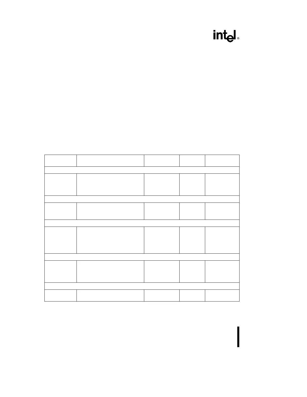
Table 4-1. Pin Summary
Pin Name Function Active State
Input/ Referenced
Output To...
Execution Control
CPUCLK2 Microprocessor Clock2 I
NUMCLK2 Math CoProcessor Clock2 I
CKM Math CoProcessor Clock Mode I
RESETIN System Reset High I CPUCLK2
Math CoProcessor Handshake
PEREQ Processor Request High O CPUCLK2
BUSY
Ý
Busy Status Low O CPUCLK2
ERROR
Ý
Error Status Low O NUMCLK2
Bus Interface
D15–D0 Data Pins I/O CPUCLK2
W/R
Ý
Write/Read Bus Cycle High/Low I CPUCLK2
ADS
Ý
Address Strobe Low I CPUCLK2
READY
Ý
Bus Ready Input Low I CPUCLK2
READYO
Ý
Ready Output Low O CPUCLK2
Chip/Port Select
STEN Status Enable High I CPUCLK2
NPS1
Ý
Numerics Select
Ý
1 Low I CPUCLK2
NPS2 Numerics Select
Ý
2 High I CPUCLK2
CMD0
Ý
Command Low I CPUCLK2
Power and Ground
V
CC
System Power
V
SS
System Ground
22
22