Philips Semiconductors Linear Products Product specification
ADC0803/4-1CMOS 8-bit A/D converters
August 31, 1994
557
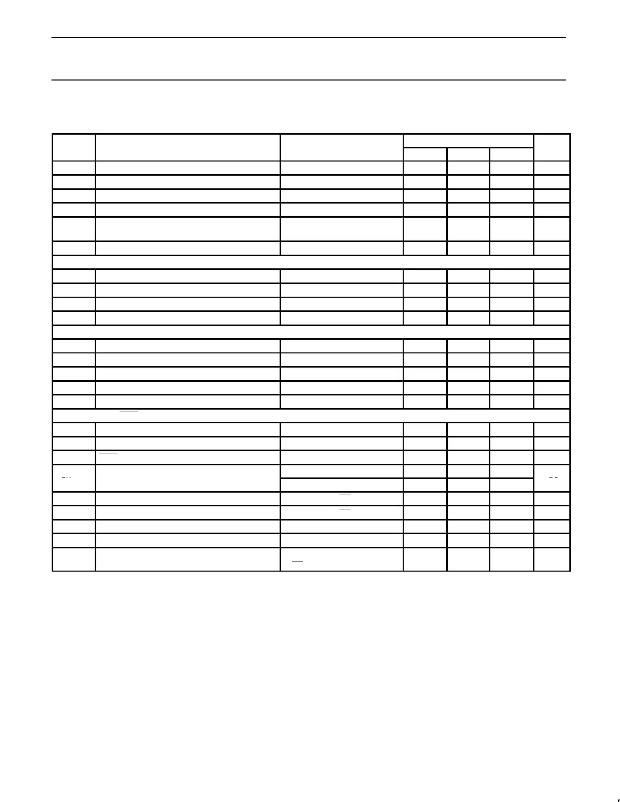
DC ELECTRICAL CHARACTERISTICS
V
CC
= 5.0V, f
CLK
= 1MHz, T
MIN
≤ T
A
≤ T
MAX
, unless otherwise specified.
ADC0803 relative accuracy error (adjusted) Full-Scale adjusted 0.50 LSB
ADC0804 relative accuracy error (unadjusted) V
REF
/2 = 2.500V
DC
1 LSB
R
IN
V
REF
/2 input resistance
3
V
CC
= 0V
2
400 680 Ω
Analog input voltage range
3
–0.05 V
CC
+0.05 V
DC common-mode error
Over analog input voltage
range
1/16 1/8 LSB
Power supply sensitivity V
CC
= 5V ±10%
1
1/16 LSB
Control inputs
V
IH
Logical “1” input voltage V
CC
= 5.25V
DC
2.0 15 V
DC
V
IL
Logical “0” input voltage V
CC
= 4.75V
DC
0.8 V
DC
I
IH
Logical “1” input current V
IN
= 5V
DC
0.005 1 µA
DC
I
IL
Logical “0” input current V
IN
= 0V
DC
–1 –0.005 µA
DC
Clock in and clock R
V
T
+ Clock in positive-going threshold voltage 2.7 3.1 3.5 V
DC
V
T
– Clock in negative-going threshold voltage 1.5 1.8 2.1 V
DC
V
H
Clock in hysteresis (V
T
+)–(V
T
–) 0.6 1.3 2.0 V
DC
V
OL
Logical “0” clock R output voltage I
OL
= 360µA, V
CC
= 4.75V
DC
0.4 V
DC
V
OH
Logical “1” clock R output voltage I
OH
= –360µA, V
CC
= 4.75V
DC
2.4 V
DC
Data output and INTR
V
OL
Logical “0” output voltage
Data outputs I
OL
= 1.6mA, V
CC
= 4.75V
DC
0.4 V
DC
INTR outputs I
OL
= 1.0mA, V
CC
= 4.75V
DC
0.4 V
DC
I
OZL
3-state output leakage V
OUT
= 0V
DC
, CS = logical “1” –3 µA
DC
I
OZH
3-state output leakage V
OUT
= 5V
DC
, CS = logical “1” 3 µA
DC
I
SC
+Output short-circuit current V
OUT
= 0V, T
A
= 25°C 4.5 12 mA
DC
I
SC
–Output short-circuit current V
OUT
= V
CC
, T
A
= 25°C 9.0 30 mA
DC
I
CC
Power supply current
f
CLK
= 1MHz, V
REF
/2 = OPEN,
CS
= Logical “1”, T
A
= 25°C
3.0 3.5 mA
NOTES:
1. Analog inputs must remain within the range: –0.05 ≤ V
IN
≤ V
CC
+ 0.05V.
2. See typical performance characteristics for input resistance at V
CC
= 5V.
3. V
REF
/2 and V
IN
must be applied after the V
CC
has been turned on to prevent the possibility of latching.