Philips Semiconductors Product specification
80C31/80C32
80C51 8-bit microcontroller family
128/256 byte RAM ROMless low voltage (2.7V–5.5V),
low power, high speed (33 MHz)
2000 Aug 07
23
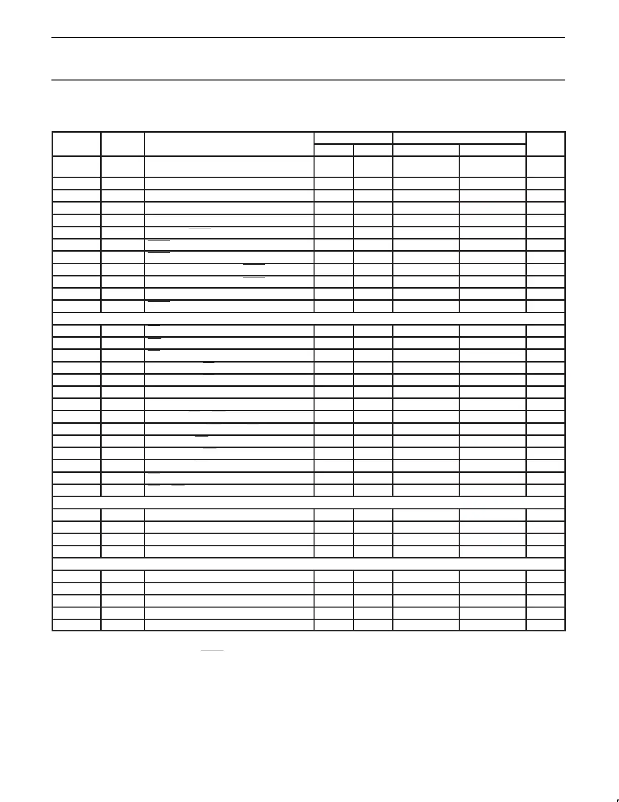
AC ELECTRICAL CHARACTERISTICS
T
amb
= 0°C to +70°C or –40°C to +85°C, V
CC
= +2.7 V to +5.5 V, V
SS
= 0 V
1,
2,
3
16 MHz CLOCK VARIABLE CLOCK
SYMBOL FIGURE PARAMETER MIN MAX MIN MAX UNIT
1/t
CLCL
14 Oscillator frequency
5
Speed versions :S
3.5 16 MHz
t
LHLL
14 ALE pulse width 85 2t
CLCL
–40 ns
t
AVLL
14 Address valid to ALE low 22 t
CLCL
–40 ns
t
LLAX
14 Address hold after ALE low 32 t
CLCL
–30 ns
t
LLIV
14 ALE low to valid instruction in 150 4t
CLCL
–100 ns
t
LLPL
14 ALE low to PSEN low 32 t
CLCL
–30 ns
t
PLPH
14 PSEN pulse width 142 3t
CLCL
–45 ns
t
PLIV
14 PSEN low to valid instruction in 82 3t
CLCL
–105 ns
t
PXIX
14 Input instruction hold after PSEN 0 0 ns
t
PXIZ
14 Input instruction float after PSEN 37 t
CLCL
–25 ns
t
AVIV
4
14 Address to valid instruction in 207 5t
CLCL
–105 ns
t
PLAZ
14 PSEN low to address float 10 10 ns
Data Memory
t
RLRH
15, 16 RD pulse width 275 6t
CLCL
–100 ns
t
WLWH
15, 16 WR pulse width 275 6t
CLCL
–100 ns
t
RLDV
15, 16 RD low to valid data in 147 5t
CLCL
–165 ns
t
RHDX
15, 16 Data hold after RD 0 0 ns
t
RHDZ
15, 16 Data float after RD 65 2t
CLCL
–60 ns
t
LLDV
15, 16 ALE low to valid data in 350 8t
CLCL
–150 ns
t
AVDV
15, 16 Address to valid data in 397 9t
CLCL
–165 ns
t
LLWL
15, 16 ALE low to RD or WR low 137 239 3t
CLCL
–50 3t
CLCL
+50 ns
t
AVWL
15, 16 Address valid to WR low or RD low 122 4t
CLCL
–130 ns
t
QVWX
15, 16 Data valid to WR transition 13 t
CLCL
–50 ns
t
WHQX
15, 16 Data hold after WR 13 t
CLCL
–50 ns
t
QVWH
16 Data valid to WR high 287 7t
CLCL
–150 ns
t
RLAZ
15, 16 RD low to address float 0 0 ns
t
WHLH
15, 16 RD or WR high to ALE high 23 103 t
CLCL
–40 t
CLCL
+40 ns
External Clock
t
CHCX
18 High time 20 20 t
CLCL
–t
CLCX
ns
t
CLCX
18 Low time 20 20 t
CLCL
–t
CHCX
ns
t
CLCH
18 Rise time 20 20 ns
t
CHCL
18 Fall time 20 20 ns
Shift Register
t
XLXL
17 Serial port clock cycle time 750 12t
CLCL
ns
t
QVXH
17 Output data setup to clock rising edge 492 10t
CLCL
–133 ns
t
XHQX
17 Output data hold after clock rising edge 8 2t
CLCL
–117 ns
t
XHDX
17 Input data hold after clock rising edge 0 0 ns
t
XHDV
17 Clock rising edge to input data valid 492 10t
CLCL
–133 ns
NOTES:
1. Parameters are valid over operating temperature range unless otherwise specified.
2. Load capacitance for port 0, ALE, and PSEN
= 100 pF, load capacitance for all other outputs = 80 pF.
3. Interfacing the 80C31 and 80C32 to devices with float times up to 45ns is permitted. This limited bus contention will not cause damage to
Port 0 drivers.
4. See application note AN457 for external memory interface.
5. Parts are guaranteed to operate down to 0 Hz. When an external clock source is used, the RST pin should be held high for a minimum of
20 µs for power-on or wakeup from power down.