Home
Intel
Timer
8253
Page 136
Intel 8253 - Page 136
773 pages
Manual
Save Page as PDF
To Next Page
To Next Page
To Previous Page
To Previous Page
Loading...
Philips Semiconductors
Product specification
80C31/80C32
80C51 8-bit microcontroller family
128/256 byte RAM ROMless low voltage (2.7V–5.5V),
low power
, high speed (33 MHz)
2000 Aug 07
30
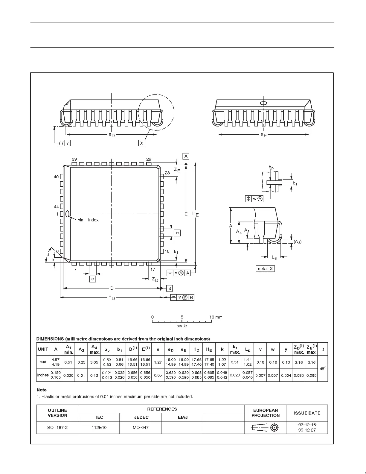
PLCC44:
plastic leaded chip carrier; 44 leads
SOT187-2
135
137
Table of Contents
Main Page
Intel387
31
Table of Contents
31
1 Pin Description Table
35
0 Functional Description
36
1 Feature List
36
2 Math Coprocessor Architecture
36
3 Power Management
37
3 1 Dynamic Mode
37
3 2 Idle Mode
37
4 Compatibility
37
5 Performance
37
1 2 Arithmetic Instructions
38
1 Instruction Set
38
1 1 Data Transfer Instructions
38
0 Programming Interface
38
1 3 Comparison Instructions
39
1 4 Transcendental Instructions
39
1 5 Load Constant Instructions
39
Figure 1-1 Intel387 SX Math
39
1 6 Processor Instructions
40
2 Register Set
40
Register Set
40
2 1 Status Word (SW) Register
41
Table 3-1 Condition Code Interpretation
42
Table 3-2 Condition Code Interpretation after FPREM and FPREM1 Instructions
43
Table 3-3 Condition Code Resulting from Comparison
43
Table 3-4 Condition Code Defining Operand Class
43
Table 3-5 Mapping Condition Codes to
43
2 2 Control Word (CW) Register
44
2 3 Data Register
45
2 4 Tag Word (TW) Register
45
2 5 Instruction and Data Pointers
45
Figure 3-4 Tag Word Register
45
Figure 3-7 Instruction and Data Pointer Image in Memory 32-Bit Real Mode Format
46
Figure 3-5 Instruction and Data Pointer Image in Memory 32-Bit Protected Mode Format
46
Figure 3-6 Instruction and Data Pointer Image in Memory 16-Bit Protected Mode Format
46
Figure 2-1 Intel387 SX Math
46
3 Data Types
47
4 Interrupt Description
47
5 Exception Handling
47
Figure 3-8 Instruction and Data Pointer Image in Memory 16-Bit Real Mode Format
47
Table 3-6 Intel387 SX Math Coprocessor Data Type Representation in Memory
48
Table 3-7 CPU Interrupt Vectors
49
0 Hardware System Interface
50
8 Programming Support
50
7 Processing Modes
50
SX Math Coprocessor
50
6 Initialization
50
1 Signal Description
51
1 1 Intel386 CPU Clock
51
Cpuclk2
51
1 2 Intel387 Math Coprocessor
51
Table 4-1 Pin Summary
51
1 8 Data Pins (D15 -D0)
52
Intel387 SX Math
52
1 10 Address Stobe (ADS )
52
1 9 Write Read Bus Cycle (W R )
52
1 5 Processor Request (PEREQ)
52
1 7 Error Status (ERROR )
52
1 6 Busy Status (BUSY )
52
1 4 System Reset (RESETIN)
52
1 3 Clocking Mode (CKM)
52
Clock 2 (NUMCLK2)
52
Table 3-8 Intel387 SX Math
53
Configuration
53
1 18 System Ground (VSS )
53
1 16 Command (CMD0 )
53
(Nps1 )
53
(Nps2)
53
1 14 Math Coprocessor Select
53
1 13 Status Enable (STEN)
53
1 12 Ready Output (READYO )
53
1 11 Bus Ready Input (READY )
53
2 System Configuration
54
Table 4-3 Bus Cycle Definition
55
4 Bus Cycles
55
3 4 Power Management Unit
55
3 3 Floating Point Unit
55
3 2 Data Interface and Control Unit
55
3 1 Bus Control Logic
55
3 Math Coprocessor Architecture
55
4 1 Intel387 SX Math Coprocessor Addressing
56
4 2 CPU Math Coprocessor Synchronization
56
4 3 Synchronous Asynchronous Modes
56
4 4 Automatic Bus Cycle Termination
56
0 Bus Operation
56
1 Non-Pipelined Bus Cycles
57
1 1 Write Cycle
57
Figure 5-1 Bus State Diagram
57
Figure 5-2 Non-Pipelined Read and Write Cycles
58
1 2 Read Cycle
58
2 Pipelined Bus Cycles
58
3 Mixed Bus Cycles
59
Figure 5-4 Pipelined Cycles with Wait States
60
4 BUSY and PEREQ Timing Relationship
61
1 Absolute Maximum Ratings
62
Table 6-2 Maximum T a at Various Airflows
62
Table 6-1 Thermal Resistances ( C Watt) I JC and I JA
62
0 Electrical Characteristics
62
2 Thermal Specifications
62
1 Mechanical Specifications
62
0 Package Specifications
62
2 D C Characteristics
63
Table 7-1 D C Specifications
63
3 A C Characteristics
64
Table 7-2A Timing Requirements of the Bus Interface Unit
64
Table 7-2B Timing Requirements of the Execution Unit
65
Table 7-2C Other AC Parameters
65
Figure 7-1A Typical Output Valid Delay Vs Load Capacitance at Max Operating Temperature
66
Figure 7-1B Typical Output Slew Time Vs Load Capacitance at Max Operating Temperature
66
Figure 7-1C Maximum ICC Vs
66
Figure 7-3 Output Signals
67
Figure 7-2 CPUCLK2 NUMCLK2
67
Figure 7-4 Input and I O Signals
68
Figure 7-5 RESET Signal
68
Figure 7-6 Float from STEN
69
Figure 7-7 Other Parameters
69
0 Intel387 SX MATH COPROCESSOR INSTRUCTION SET
70
Table 8-1 Instruction Formats
70
Appendix Aintel387 Sx Math Coprocessor Compatibility
74
A 1 8087 80287 Compatibility
74
A 1 1 General Differences
74
A 1 2 Exceptions
75
Appendix B Compatibility
76
Math Coprocessor
77
Programming Interface
79
Register Set
80
Data Registers
80
Figure 3-2 Status Word
81
Exception Handling
85
General Differences
87
Hardware Interface
90
Signal Description
90
Processor Architecture
92
Floating-Point Unit
93
Bus Cycles
93
Bus Operation
94
System Configuration
95
Electrical Data
97
Clock Timings
99
Integrated Circuits
107
Selection Table
108
Block Diagram
110
Pin Configurations
111
Pin Descriptions
112
Oscillator Characteristics
114
Program Memory
114
Symbol Function
124
Ac Electrical Characteristics
126
DC Electrical Characteristics
127
Programmable Interval Timer
139
Data Bus Buffer
140
Control Word Register
141
System Interface
143
Counter Latch Command
145
Read-Back Command
146
Mode 0 Interrupt on Terminal Count
148
Mode 2 Rate Generator
148
Mode 1 Hardware Retriggerable One-Shot
148
Mode 4 Software Triggered Strobe
153
Mode 5 Hardware Triggered Strobe
154
Read Cycle
156
Write Cycle
157
Frequency
160
Functional Description
161
Block Diagram
162
Operational Description
164
Control Word Format
164
Write Operations
165
Read Operations
165
Mode Definitions
168
Absolute Maximum Ratings
174
Revision Summary
177
Ordering Information
179
Functional Diagram
179
Pin Description
179
Functional Description
180
Diagram
181
Figure 3-3 Control Word
182
Max Count
189
Timing Waveforms
192
Basic Concepts
196
Input Output
210
Signal to Noise Ratio (SNR)
214
Offset Errors
221
Typical Applications
246
AC Electrical Characteristics
247
Power Supply
248
Typical Performance Characteristics
249
Timing Diagrams
250
Functional Description
260
General Applications
273
Physical Dimensions
284
Life Support Policy
285
Block Diagram
287
DC Electrical Characteristics
288
Ac Electrical Characteristics
289
Analog Operation
289
Typical Performance Characteristics
293
Section 2
301
Introduction and Reading Guide
302
Development of MS-DOS* Mode with 80286 and 80287; Intel386™ Processor and Intel387 Math Coprocessor
303
Intel387 Math Coprocessor
303
Ms-Dos* Compatible Handlers and
303
Special Hardware for the 80287 Interface
304
Special Hardware for the Intel387 Math Coprocessor Interface
304
Basic Rules: When Ferr# Is Generated
305
FERR# & IGNNE# with Intel486™ and
305
Recommended External Hardware to Support Ms-Dos* Compatibility
306
Pentium ® Pro Processor with
308
Wait" Fpu Instructions Can Get Fpu Interrupt in Window
308
Numeric Exceptions and Their Defaults
312
Recommended Protocol for Ms-Dos ™ and Windows* 95 Compatible Handlers
312
Two Options for Handling Numeric Exceptions
312
Automatic Exception Handling : Using Masked Exceptions
313
Software Exception Handling
314
Exception Synchronization Examples
315
Exception Synchronization: What, Why and When
315
Synchronization Required for Use of FPU Exception Handlers
315
FPU Exception Handling Examples
316
Proper Exception Synchronization in General
316
Considerations When FPU Shared between Tasks
320
Need for Preserving the State of IGNNE# Circuit if Use FPU and SMM
320
Speculatively Deferring Fpu Saves, General Overview
321
Interaction of Fpu State Saves and Fp Exception Association
322
Tracking Fpu Ownership
322
Interrupt Routing from the Kernel
324
Changes with Intel486 ™ , Pentium
325
Considerations When FPU Shared between Tasks Using Native Mode
325
Life Support Applications
328
Data Processing
330
Architectural Overview
331
Memory Organization
331
Register File
331
Special Function Registers
335
Core Registers
337
Execution Unit
338
Interrupt Controller
338
Debugging Features
340
Task Management
341
Instruction Set
342
Instruction Syntax
342
Instruction Set Summary
345
Other Instructions
347
External Bus
348
Bus Timing
349
Software Compatibility
352
Hardware Compatibility
352
Data Memory
359
Data Memory Addressing
360
Indirect Addressing
362
Bit Address
362
Direct Addressing
363
SFR Addressing
363
Bit Addressing
363
Special Function Registers (Sfrs)
366
Program Status Word
370
System Configuration Register
373
Power-Up Reset
375
Startup Code
379
Using an External Clock
380
Power Control
380
Idle Mode
381
Power down Mode
381
PUSH and POP
382
Stack Overflow
384
Service Precedence
388
Software Interrupt
389
Fixed Priority
389
Interrupt Stack Frame
392
Interrupt Vector Table
393
Register Banks
398
Addressing Modes
401
Description of the Modes
402
Register File
402
Immediate Addressing
406
Immediate Data
406
Instruction Set Overview
409
Operation
456
Operation
508
Operation
531
Software Reset
546
Return from Interrupt
548
Rotate Left
549
Rotate Right
551
Address Lines
578
Bus Configuration
579
Reset Configuration
591
I/O Port Access
592
Open Drain Output
595
Push-Pull Output
595
Compatibility Considerations
599
On-Chip Peripherals
602
Bus Interface
602
Pin Description
618
Hardware Description
621
Clock Waveforms
633
Ordering Information
634
Operating Modes
639
Control Word
640
Timing Waveforms
653
Functional Description
663
Special Mask Mode
670
Application Note
682
DC Electrical Characteristics
697
Test Circuits
712
Typical Application
716
Programming Devices
724
Hardware Interrupts
730
Memory Mapped I/O
743
Differences for Handlers Using Native Mode
325
Origin with 80286 and 80287; Intel386™ Processor and Intel387 Math Coprocessor
325
Pro Processors with CR0.NE=1
325
Section 3
750
Precautionary Measures
753
Before You Begin
754
Recording the System Configuration
754
Updating the BIOS
754
Updating the ESM Firmware
754
Installing Upgrade Microprocessors in the Poweredge 1300
755
Saving RCU Configuration Settings
755
Installing Upgrade Microprocessors in the Poweredge 2300
757
Installing Upgrade Microprocessors in the Poweredge 2400
759
Installing Upgrade Microprocessors in the Poweredge 4300
761
Installing Upgrade Microprocessors in the Poweredge 4350
764
Removing the Microprocessors
765
Removing and Replacing the Guide Brackets
766
Removing and Replacing the Cooling Shroud
768
Removing the Cooling Shroud
768
Installing the Upgrade Microprocessor
769
Replacing the Cooling Shroud
769
Installing a New Cooling Shroud
771
Reassembling and Checking the System
771