4-1
Semiconductor
March 1997
82C54
CMOS Programmable Interval Timer
Features
• 8MHz to 12MHz Clock Input Frequency
• Compatible with NMOS 8254
- Enhanced Version of NMOS 8253
• Three Independent 16-Bit Counters
• Six Programmable Counter Modes
• Status Read Back Command
• Binary or BCD Counting
• Fully TTL Compatible
• Single 5V Power Supply
• Low Power
- ICCSB . . . . . . . . . . . . . . . . . . . . . . . . . . . . . . . . . .10µA
- ICCOP . . . . . . . . . . . . . . . . . . . . . . . . . .10mA at 8MHz
• Operating Temperature Ranges
- C82C54 . . . . . . . . . . . . . . . . . . . . . . . . . .0
o
C to +70
o
C
- I82C54 . . . . . . . . . . . . . . . . . . . . . . . . . -40
o
C to +85
o
C
- M82C54 . . . . . . . . . . . . . . . . . . . . . . . -55
o
C to +125
o
C
Description
The Harris 82C54 is a high performance CMOS Programma-
ble Interval Timer manufactured using an advanced 2 micron
CMOS process.
The 82C54 has three independently programmable and
functional 16-bit counters, each capable of handling clock
input frequencies of up to 8MHz (82C54) or 10MHz
(82C54-10) or 12MHz (82C54-12).
The high speed and industry standard configuration of the
82C54 make it compatible with the Harris 80C86, 80C88,
and 80C286 CMOS microprocessors along with many other
industry standard processors. Six programmable timer
modes allow the 82C54 to be used as an event counter,
elapsed time indicator, programmable one-shot, and many
other applications. Static CMOS circuit design insures low
power operation.
The Harris advanced CMOS process results in a significant
reduction in power with performance equal to or greater than
existing equivalent products.
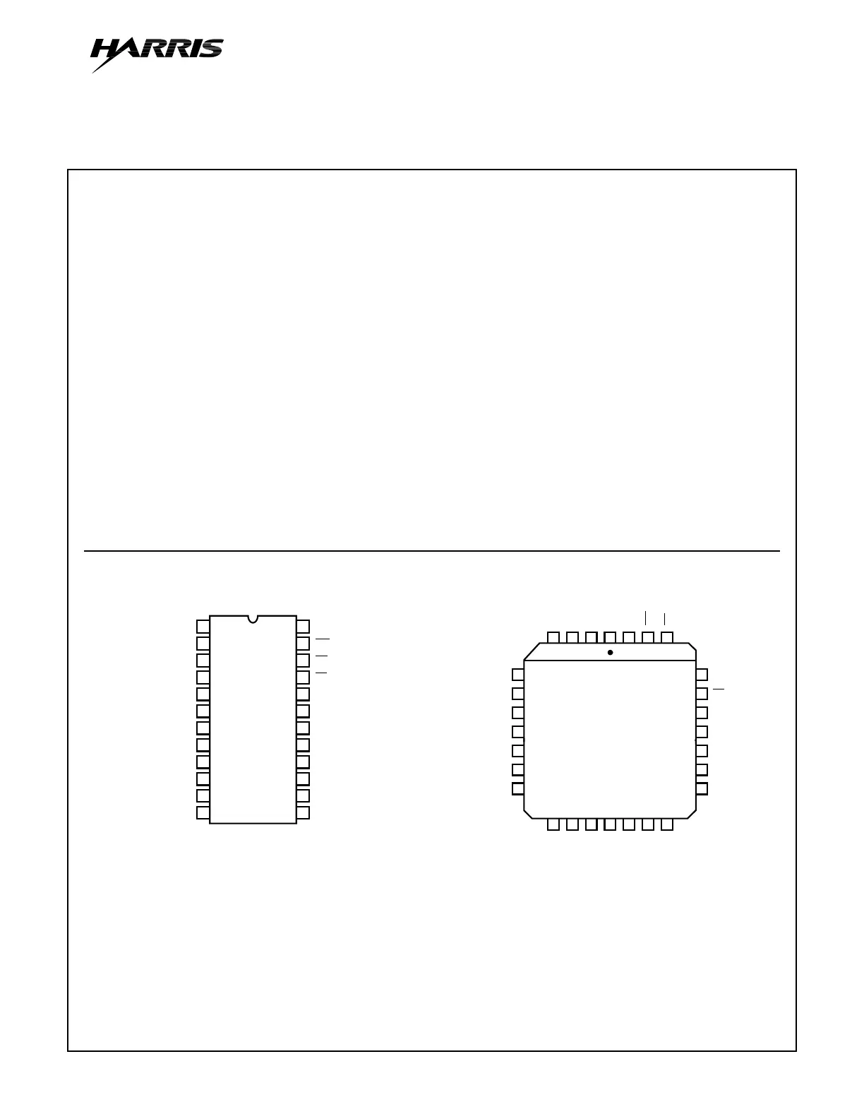
Pinouts
82C54 (PDIP, CERDIP, SOIC)
TOP VIEW
82C54 (PLCC/CLCC)
TOP VIEW
1
2
3
4
5
6
7
8
9
10
11
12
16
17
18
19
20
21
22
23
24
15
14
13
D7
D6
D5
D4
D3
D2
D1
D0
CLK 0
OUT 0
GATE 0
GND
VCC
RD
CS
A1
A0
OUT 2
CLK 1
GATE 1
OUT 1
WR
CLK 2
GATE 2
GND
NC
OUT 1
GATE 1
CLK 1
OUT 0
GATE 0
D7
NC
VCC
WR
RD
D5
D6
CS
A1
A0
CLK2
NC
GATE 2
OUT 2
1234
5
6
7
8
9
10
11
12 13 14 15 16 17 18
19
20
21
22
23
24
25
262728
D3
D2
D1
D0
D4
NC
CLK 0
CAUTION: These devices are sensitive to electrostatic discharge. Users should follow proper IC Handling Procedures.
Copyright
© Harris Corporation 1997
File Number 2970.1