Functional Description (Continued)
2.2 Analog Differential Voltage Inputs and
Common-Mode Rejection
This A/D has additional applications flexibility due to the ana-
log differential voltage input. The V
IN
(−) input (pin 7) can be
used to automatically subtract a fixed voltage value from the
input reading (tare correction). This is also useful in 4 mA–20
mA current loop conversion. In addition, common-mode
noise can be reduced by use of the differential input.
The time interval between sampling V
IN
(+) and V
IN
(−) is 4-
1
⁄
2
clock periods. The maximum error voltage due to this slight
time difference between the input voltage samples is given
by:
where:
∆V
e
is the error voltage due to sampling delay
V
P
is the peak value of the common-mode voltage
f
cm
is the common-mode frequency
As an example, to keep this error to
1
⁄
4
LSB (∼5 mV) when
operating with a 60 Hz common-mode frequency, f
cm
, and
using a 640 kHz A/D clock, f
CLK
, would allow a peak value of
the common-mode voltage, V
P
, which is given by:
or
which gives
V
P
≅
1.9V.
The allowed range of analog input voltages usually places
more severe restrictions on input common-mode noise lev-
els.
An analog input voltage with a reduced span and a relatively
large zero offset can be handled easily by making use of the
differential input (see section 2.4 Reference Voltage).
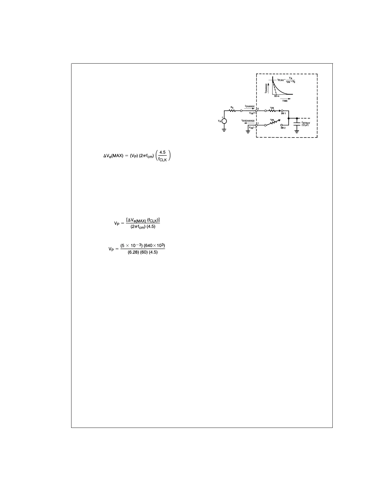
2.3 Analog Inputs
2.3 1 Input Current
Normal Mode
Due to the internal switching action, displacement currents
will flow at the analog inputs. This is due to on-chip stray ca-
pacitance to ground as shown in
Figure 5
.
The voltage on this capacitance is switched and will result in
currents entering the V
IN
(+) input pin and leaving the V
IN
(−)
input which will depend on the analog differential input volt-
age levels. These current transients occur at the leading
edge of the internal clocks. They rapidly decay and
do not
cause errors
as the on-chip comparator is strobed at the end
of the clock period.
Fault Mode
If the voltage source applied to the V
IN
(+) or V
IN
(−) pin ex-
ceeds the allowed operating range of V
CC
+50 mV, large in-
put currents can flow through a parasitic diode to the V
CC
pin. If these currents can exceed the 1 mA max allowed
spec, an external diode (1N914) should be added to bypass
this current to the V
CC
pin (with the current bypassed with
this diode, the voltage at the V
IN
(+) pin can exceed the V
CC
voltage by the forward voltage of this diode).
2.3.2 Input Bypass Capacitors
Bypass capacitors at the inputs will average these charges
and cause a DC current to flow through the output resis-
tances of the analog signal sources. This charge pumping
action is worse for continuous conversions with the V
IN
(+) in-
put voltage at full-scale. For continuous conversions with a
640 kHz clock frequency with the V
IN
(+) input at 5V, this DC
current is at a maximum of approximately 5 µA. Therefore,
bypass capacitors should not be used at the analog inputs or
the V
REF
/2 pin
for high resistance sources (
>
1kΩ). If input
bypass capacitors are necessary for noise filtering and high
source resistance is desirable to minimize capacitor size, the
detrimental effects of the voltage drop across this input resis-
tance, which is due to the average value of the input current,
can be eliminated with a full-scale adjustment while the
given source resistor and input bypass capacitor are both in
place. This is possible because the average value of the in-
put current is a precise linear function of the differential input
voltage.
2.3.3 Input Source Resistance
Large values of source resistance where an input bypass ca-
pacitor is not used,
will not cause errors
as the input currents
settle out prior to the comparison time. If a low pass filter is
required in the system, use a low valued series resistor
(≤ 1kΩ) for a passive RC section or add an op amp RC ac-
tive low pass filter. For low source resistance applications,
(≤ 1kΩ), a 0.1 µF bypass capacitor at the inputs will prevent
noise pickup due to series lead inductance of a long wire. A
DS005671-14
r
ON
of SW 1 and SW 2
≅
5kΩ
r
=
r
ON
C
STRAY
≅
5kΩx12pF
=
60 ns
FIGURE 5. Analog Input Impedance
ADC0801/ADC0802/ADC0803/ADC0804/ADC0805
www.national.com 20