80C187
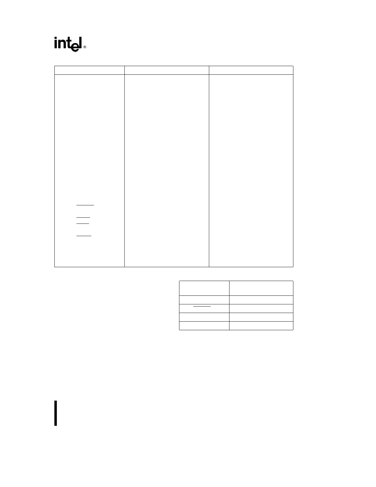
Table 8. PLCC Pin Cross-Reference
Pin Name CERDIP Package PLCC Package
BUSY 25 28
CKM 39 44
CLK 32 36
CMD0 29 32
CMD1 31 35
D
0
23 26
D
1
22 25
D
2
21 24
D
3
20 22
D
4
19 21
D
5
18 20
D
6
17 19
D
7
16 18
D
8
15 17
D
9
14 16
D
10
12 14
D
11
11 13
D
12
89
D
13
78
D
14
67
D
15
55
ERROR
26 29
No Connect 2 6, 11, 23, 33, 40
NPRD
27 30
NPS1
34 38
NPS2 33 37
NPWR
28 31
PEREQ 24 27
RESET 35 39
V
CC
3, 9, 13, 37, 40 1, 3, 10, 15, 42
V
SS
1, 4, 10, 30, 36, 38 2, 4, 12, 34, 41, 43
System Reset (RESET)
A LOW to HIGH transition on this pin causes the
80C187 to terminate its present activity and to enter
a dormant state. RESET must remain active (HIGH)
for at least four internal clock periods. (The relation
of the internal clock period to CLK depends on
CLKM; the internal clock may be different from that
of the CPU.) Note that the 80C187 is active internal-
ly for 25 clock periods after the termination of the
RESET signal (the HIGH to LOW transition of RE-
SET); therefore, the first instruction should not be
written to the 80C187 until 25 internal clocks after
the falling edge of RESET. Table 9 shows the status
of the output pins during the reset sequence. After a
reset, all output pins return to their inactive states.
Table 9. Output Pin Status during Reset
Output Value
Pin Name during Reset
BUSY HIGH
ERROR HIGH
PEREQ LOW
D
15
–D
0
TRI-STATE OFF
Processor Extension Request (PEREQ)
When active, this pin signals to the CPU that the
80C187 is ready for data transfer to/from its data
FIFO. When there are more than five data transfers,
15