EasyManua.ls Logo

Lattice Semiconductor CertusPro-NX - Serdes;Pcs Block Latency; Table 12.1. Transmit;Receive Serdes;Pcs Latency

Default Icon
171 pages
To Next Page IconTo Next Page
To Previous Page IconTo Previous Page
Loading...
CertusPro-NX SerDes/PCS Usage Guide
Preliminary Technical Note
FPGA-TN-02245-0.81 © 2020-2021 Lattice Semiconductor 105
All rights reserved. CONFIDENTIAL
SerDes/PCS Block Latency
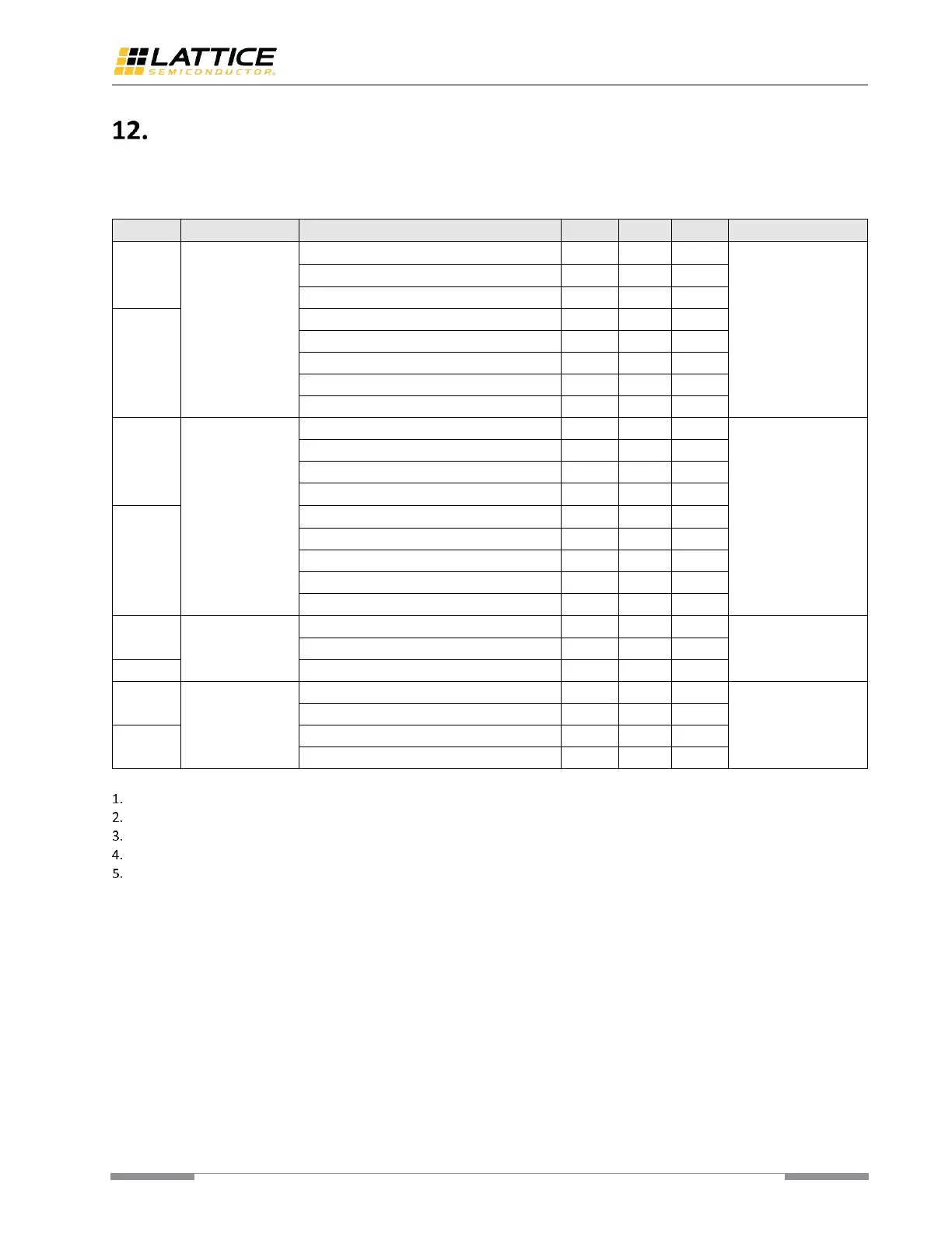
Table 12.1 provides transmit and receive latencies respectively in the SerDes, as well as different stages inside the PCS.
The latency is in number of parallel word clocks.
Table 12.1. Transmit/Receive SerDes/PCS Latency
Tx/Rx
SerDes/PCS
Mode
Description
Bypass
Min
Max
Unit
Tx Path
8B/10B PCS
Tx Interface FIFO
2
8
12
EPCS clock
8B/10B Encoder
1
1
1
Phase Matching FIFO
1
1
7
11
Rx Path
Word Aligner
1
1
3
8B/10B Decoder
1
1
1
Lane Aligner
1
1
5
10
2
Clock Compensation FIFO
1
16
20
Rx Interface FIFO
2
8
12
Tx Path
64B/66B PCS
Tx Interface FIFO
1
4
9
EPCS div4 clock
64B66B Encoder
1
3
3
Scrambler
1
1
1
Tx Gear Box
N/A
2
3
3
4
Rx Path
Block Aligner
1
1
1
Descrambler
1
1
1
64B66B Decoder
1
3
3
Rx Interface FIFO (with CTC functionality)
2
10
12
Rx Gear Box
N/A
2
3
3
4
Tx Path
PMA Only
Tx Interface FIFO
2
8
12
EPCS clock
Phase Matching FIFO
1
1
7
11
Rx Path
Rx Interface FIFO
2
8
12
Tx Path
SerDes/PMA
Serializer
N/A
3
4
UI
Gearing Box
N/A
2
2
Rx Path
Deserializer
N/A
4
5
Gearing Box
N/A
1
5
1
5
Notes:
Enabled in multi-lane mode. Otherwise, disabled.
The actual value should be added with the max_skew between two different lanes.
The actual value should be added with one EPCS clock cycle.
The actual value should be added with three ECPS clock cycles.
The actual value should be added with one EPCS clock cycle.

Table of Contents

Other manuals for Lattice Semiconductor CertusPro-NX