CertusPro-NX SerDes/PCS Usage Guide
Preliminary Technical Note
54 © 2020-2021 Lattice Semiconductor FPGA-TN-02245-0.81
All rights reserved. CONFIDENTIAL
Figure 6.7. Tx Gearing Case II
The phase compensation FIFO resolves clock phase difference between its read side and write side. The FIFO can signal
its overflow and underflow status once they happen. Write side and read side clock should not have frequency
difference. Otherwise, the FIFO overflow or underflow occurs.
The phase compensation FIFO can also be bypassed. When being bypassed, it works as synchronous D-Flip Flop (DFF)
to capture the data from fabric. Table 6.4 is the comparison between using phase compensation FIFO and bypassing
the FIFO.
Table 6.4. Tx FIFO Usage
It is robust and easy to use. Timing closure is
easy to be achieved.
Strict timing constraint must be applied to the
Fabric-MPCS interface.
Bigger and uncertain latency is introduced by
this FIFO.
Must use this mode if low latency or
deterministic latency are required
Extra lane-to-lane skew between every two
bonded channels may be introduced.
No extra lane-to-lane skew is introduced.
In the multiple-channel mode, the Tx Lane-to-lane Deskew FIFO is optionally enabled on all channels to eliminate the
lane-to-lane skew introduced by the uncertain latency of phase compensation FIFO.
Note: Refer to the 8B/10B PCS Multiple Lane Tx Path section for more details about the multiple-channel alignment
mode.
Rx FIFO
The Rx FIFO module also serves two purposes:
1:2 gearing MPCS data before forwarding to fabric.
Clock phase compensation FIFO to ease MPCS-Fabric interface timing closure.
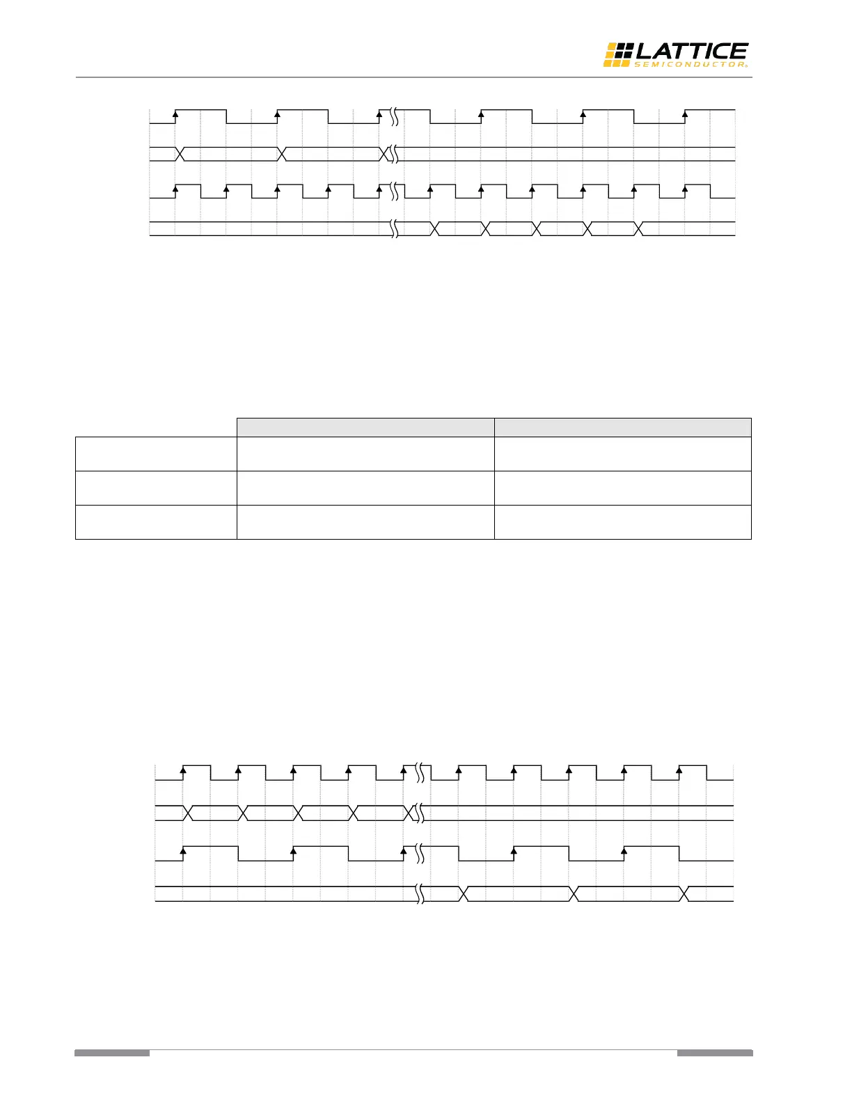
The 1:2 gearing can be optionally enabled to convert 2-byte data to 4-byte. Figure 6.8 shows how this conversion
proceeds.
Figure 6.8. Rx Gearing Case I
The 1:2 gearing logic can convert 1-byte data to 2-byte, too. Figure 6.9 shows how this conversion proceeds.
D1D0 D3D2
D0 D1 D2 D3
Wr Clock
Wr Data
Rd Clock
Rd Data
D1D0 D3D2 D5D4 D7D6
D3D2D1D0 D7D6D5D4
Wr Clock
Wr Data
Rd Clock
Rd Data
 Loading...