CertusPro-NX SerDes/PCS Usage Guide
Preliminary Technical Note
94 © 2020-2021 Lattice Semiconductor FPGA-TN-02245-0.81
All rights reserved. CONFIDENTIAL
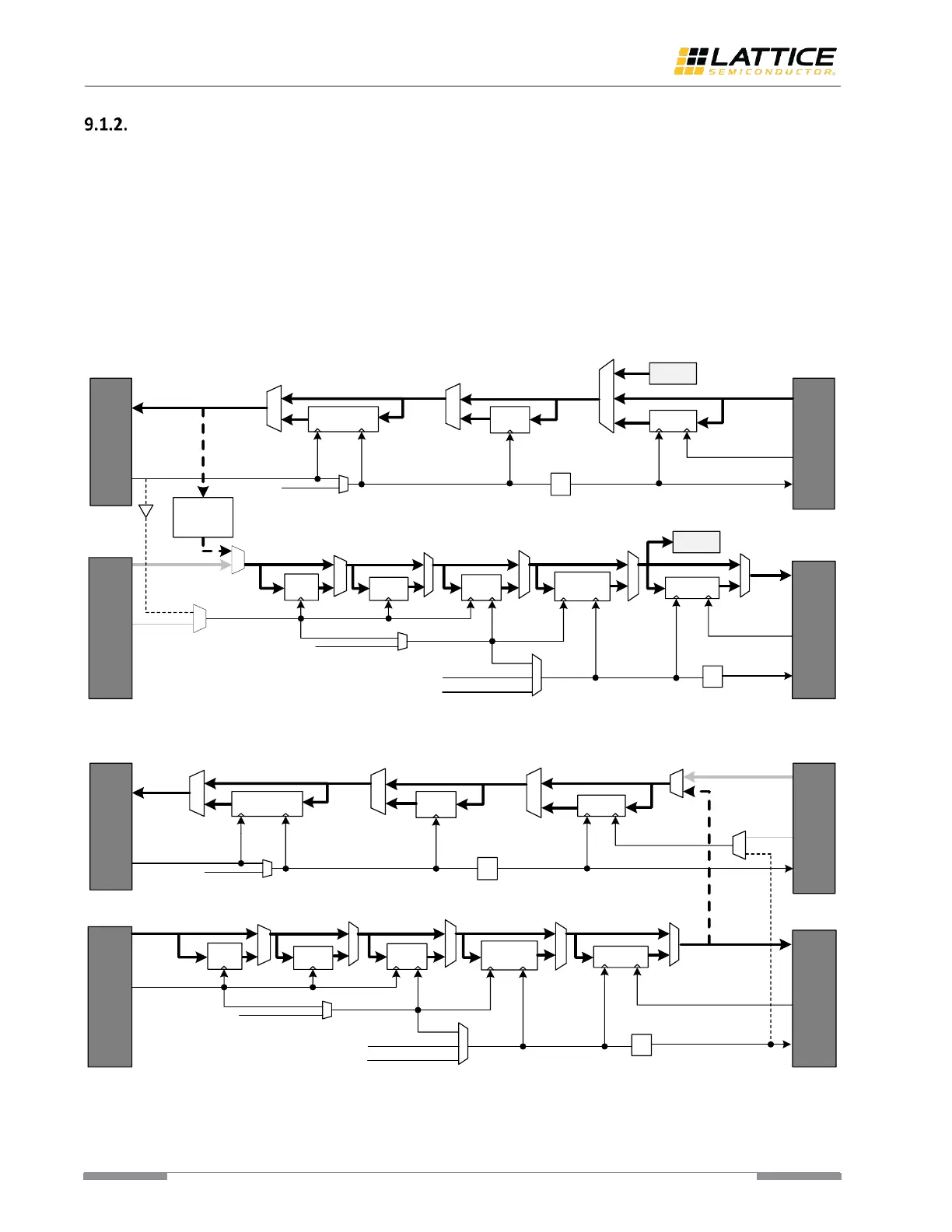
8B/10B PCS Loopback
The 8B/10B PCS implements two loopback modes, 8B/10B PCS Near-End Parallel Loopback Mode and 8B/10B PCS
Far-End Parallel Loopback Mode.
Figure 9.2 shows the block diagram of 8B/10B PCS Near-End Parallel Loopback Mode. In this mode, the 8B/10B PCS
output data passes through a phase compensation FIFO (Loopback FIFO) to Rx path. In addition, the tx_pcs_clk is used
to drive Rx path. This loopback mode can be enabled or disabled by the bit[0] of MPCS register rege0.
Figure 9.3 shows the block diagram of 8B/10B PCS Far-End Parallel Loopback Mode. In this mode, the 8B/10B PCS Rx
output data is looped back to Tx path near fabric side. In addition, the rx_out_clk is used to drive the writing side of the
Tx FIFO. What should be noted is that the Tx and Rx path clock must have no frequency difference. In other words, the
Tx path and Rx path should share the same reference clock source. This loopback mode can be enabled or disabled by
the bit[1] of MPCS register rege0.
 Loading...