CertusPro-NX SerDes/PCS Usage Guide
Preliminary Technical Note
38 © 2020-2021 Lattice Semiconductor FPGA-TN-02245-0.81
All rights reserved. CONFIDENTIAL
Other Signals
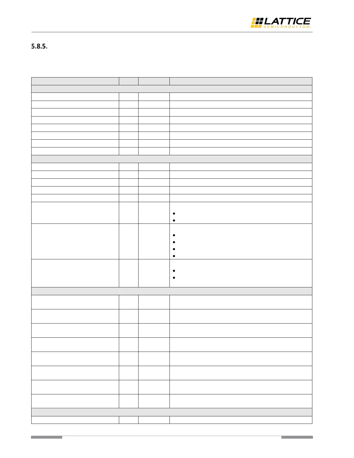
Table 5.11 shows signals other than MPCS, EPCS, PIPE and LMMI interfaces per quad. NL means the number of lanes.
For detailed descriptions about Quad-to-Quad signals, refer to the Clocks and Reset section.
Table 5.11. Other Signals
Reference Clock of SerDes PLL in one Quad.
Reference Clock of SerDes PLL in one Quad.
Analog Rx differential IO.
Analog Rx differential IO.
Analog Tx differential IO.
Analog Tx differential IO.
Analog reference return for PMA PLL.
Reference Clock from SD_EXT0_REFCLKP, SD_EXT0_REFCLKN.
Reference Clock from SD_EXT1_REFCLKP, SD_EXT1_REFCLKN.
Reference Clock from left top GPLL.
Reference Clock from right top GPLL.
Reference Clock from FPGA Fabric, only for test purpose.
Dynamic clock source selection:
1’b1 – sd_ext_1_refclk_i.
1’b0 – sd_ext_0_refclk_i.
Dynamic clock source selection:
2’b11 – sd_pll_refclk_i.
2’b10 – sd_ext_0_refclk_i or sd_ext_1_refclk_i.
2’b01 – pll_1_refclk_i.
2’b00 – pll_0_refclk_i.
Dynamic clock source selection:
1’b1 – clock from PCSREFMUX output.
1’b0 – clock from per quad source (sdq_refclkp_i,
sdq_refclkn_i).
The outputted clock for sharing among Quads are hooked up
during Quad integration.
The outputted clock for sharing among Quads are hooked up
during Quad integration.
The input clock is shared by all channels within a Quad to
implement lane alignment.
The input clock is shared by all channels within a Quad to
implement lane alignment.
The connection signals between Quads for lane alignment
across Quad boundary.
The connection signals between Quads for lane alignment
across Quad boundary.
The connection signals between Quads for lane alignment
across Quad boundary.
The connection signals between Quads for lane alignment
across Quad boundary.
When asserted, this signal activates the ACJTAG controller of
 Loading...